- 您現(xiàn)在的位置:買賣IC網(wǎng) > PDF目錄19820 > LAMXO640C-3TN100E (Lattice Semiconductor Corporation)IC FPGA AUTO 640LUTS 100TQFP PDF資料下載
參數(shù)資料
| 型號(hào): | LAMXO640C-3TN100E |
| 廠商: | Lattice Semiconductor Corporation |
| 文件頁數(shù): | 8/77頁 |
| 文件大小: | 0K |
| 描述: | IC FPGA AUTO 640LUTS 100TQFP |
| 標(biāo)準(zhǔn)包裝: | 90 |
| 系列: | LA-MachXO |
| 可編程類型: | 系統(tǒng)內(nèi)可編程 |
| 最大延遲時(shí)間 tpd(1): | 4.9ns |
| 電壓電源 - 內(nèi)部: | 1.71 V ~ 3.465 V |
| 宏單元數(shù): | 320 |
| 輸入/輸出數(shù): | 74 |
| 工作溫度: | -40°C ~ 125°C |
| 安裝類型: | 表面貼裝 |
| 封裝/外殼: | 100-LQFP |
| 供應(yīng)商設(shè)備封裝: | 100-TQFP(14x14) |
| 包裝: | 托盤 |
| 其它名稱: | 220-1639 LAMXO640C-3TN100E-ND |
第1頁第2頁第3頁第4頁第5頁第6頁第7頁當(dāng)前第8頁第9頁第10頁第11頁第12頁第13頁第14頁第15頁第16頁第17頁第18頁第19頁第20頁第21頁第22頁第23頁第24頁第25頁第26頁第27頁第28頁第29頁第30頁第31頁第32頁第33頁第34頁第35頁第36頁第37頁第38頁第39頁第40頁第41頁第42頁第43頁第44頁第45頁第46頁第47頁第48頁第49頁第50頁第51頁第52頁第53頁第54頁第55頁第56頁第57頁第58頁第59頁第60頁第61頁第62頁第63頁第64頁第65頁第66頁第67頁第68頁第69頁第70頁第71頁第72頁第73頁第74頁第75頁第76頁第77頁
2-13
Architecture
Lattice Semiconductor
LA-MachXO Automotive Family Data Sheet
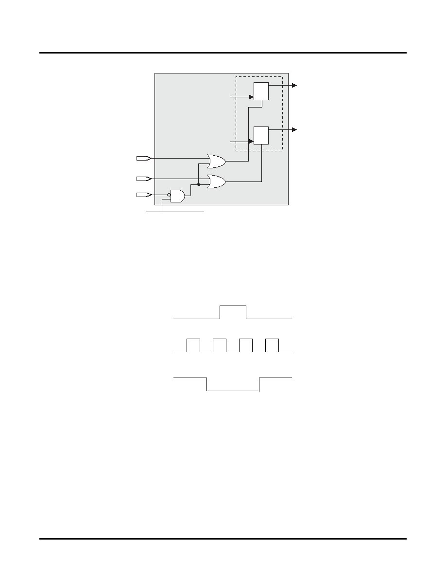
Figure 2-13. Memory Core Reset
For further information on the sysMEM EBR block, see the details of additional technical documentation at the end
of this data sheet.
EBR Asynchronous Reset
EBR asynchronous reset or GSR (if used) can only be applied if all clock enables are low for a clock cycle before the
reset is applied and released a clock cycle after the reset is released, as shown in Figure 2-14. The GSR input to the
EBR is always asynchronous.
Figure 2-14. EBR Asynchronous Reset (Including GSR) Timing Diagram
If all clock enables remain enabled, the EBR asynchronous reset or GSR may only be applied and released after
the EBR read and write clock inputs are in a steady state condition for a minimum of 1/fMAX (EBR clock). The reset
release must adhere to the EBR synchronous reset setup time before the next active read or write clock edge.
If an EBR is pre-loaded during conguration, the GSR input must be disabled or the release of the GSR during
device Wake Up must occur before the release of the device I/Os becoming active.
These instructions apply to all EBR RAM, ROM and FIFO implementations. For the EBR FIFO mode, the GSR sig-
nal is always enabled and the WE and RE signals act like the clock enable signals in Figure 2-14. The reset timing
rules apply to the RPReset input vs the RE input and the RST input vs. the WE and RE inputs. Both RST and
RPReset are always asynchronous EBR inputs.
Note that there are no reset restrictions if the EBR synchronous reset is used and the EBR GSR input is disabled.
Q
SET
D
LCLR
Output Data
Latches
Memory Core
Port A[17:0]
Q
SET
D
Port B[17:0]
RSTB
GSRN
Programmable Disable
RSTA
LCLR
Reset
Clock
Enable
相關(guān)PDF資料 |
PDF描述 |
|---|---|
| MAX8518EUB+T | IC REG LDO ADJ 1A 10-UMAX |
| RCM12DRUS | CONN EDGECARD 24POS DIP .156 SLD |
| GRM31CR60J226KE19L | CAP CER 22UF 6.3V 10% X5R 1206 |
| M4A5-64/32-7VI | IC CPLD ISP 4A 64MC 44TQFP |
| MAX6469TA15BD3+T | IC REG LDO 1.5V/ADJ .3A 8-TDFN |
相關(guān)代理商/技術(shù)參數(shù) |
參數(shù)描述 |
|---|---|
| LAMXO640C-3TN144E | 功能描述:CPLD - 復(fù)雜可編程邏輯器件 Auto Grade (AEC-Q100 ) MachXO640C RoHS:否 制造商:Lattice 系列: 存儲(chǔ)類型:EEPROM 大電池?cái)?shù)量:128 最大工作頻率:333 MHz 延遲時(shí)間:2.7 ns 可編程輸入/輸出端數(shù)量:64 工作電源電壓:3.3 V 最大工作溫度:+ 90 C 最小工作溫度:0 C 封裝 / 箱體:TQFP-100 |
| LAMXO640E | 制造商:LATTICE 制造商全稱:Lattice Semiconductor 功能描述:LA-MachXO Automotive Family Data Sheet |
| LAMXO640E-3FTN256E | 功能描述:CPLD - 復(fù)雜可編程邏輯器件 Auto Grade (AEC-Q100 ) MachXO640E RoHS:否 制造商:Lattice 系列: 存儲(chǔ)類型:EEPROM 大電池?cái)?shù)量:128 最大工作頻率:333 MHz 延遲時(shí)間:2.7 ns 可編程輸入/輸出端數(shù)量:64 工作電源電壓:3.3 V 最大工作溫度:+ 90 C 最小工作溫度:0 C 封裝 / 箱體:TQFP-100 |
| LAMXO640E-3TN100E | 功能描述:CPLD - 復(fù)雜可編程邏輯器件 Auto Grade (AEC-Q100 ) MachXO640E RoHS:否 制造商:Lattice 系列: 存儲(chǔ)類型:EEPROM 大電池?cái)?shù)量:128 最大工作頻率:333 MHz 延遲時(shí)間:2.7 ns 可編程輸入/輸出端數(shù)量:64 工作電源電壓:3.3 V 最大工作溫度:+ 90 C 最小工作溫度:0 C 封裝 / 箱體:TQFP-100 |
| LAMXO640E-3TN144E | 功能描述:CPLD - 復(fù)雜可編程邏輯器件 Auto Grade (AEC-Q100 ) MachXO640E RoHS:否 制造商:Lattice 系列: 存儲(chǔ)類型:EEPROM 大電池?cái)?shù)量:128 最大工作頻率:333 MHz 延遲時(shí)間:2.7 ns 可編程輸入/輸出端數(shù)量:64 工作電源電壓:3.3 V 最大工作溫度:+ 90 C 最小工作溫度:0 C 封裝 / 箱體:TQFP-100 |
發(fā)布緊急采購(gòu),3分鐘左右您將得到回復(fù)。