- 您現(xiàn)在的位置:買賣IC網 > PDF目錄377835 > M7040N-083ZA1T (意法半導體) CAP 5600PF 100V 10% X7R AXIAL BULK P-MIL-PRF-39014 PDF資料下載
參數(shù)資料
| 型號: | M7040N-083ZA1T |
| 廠商: | 意法半導體 |
| 英文描述: | CAP 5600PF 100V 10% X7R AXIAL BULK P-MIL-PRF-39014 |
| 中文描述: | 64K的× 72位的網絡數(shù)據(jù)包進入搜索引擎 |
| 文件頁數(shù): | 21/159頁 |
| 文件大?。?/td> | 1088K |
| 代理商: | M7040N-083ZA1T |
第1頁第2頁第3頁第4頁第5頁第6頁第7頁第8頁第9頁第10頁第11頁第12頁第13頁第14頁第15頁第16頁第17頁第18頁第19頁第20頁當前第21頁第22頁第23頁第24頁第25頁第26頁第27頁第28頁第29頁第30頁第31頁第32頁第33頁第34頁第35頁第36頁第37頁第38頁第39頁第40頁第41頁第42頁第43頁第44頁第45頁第46頁第47頁第48頁第49頁第50頁第51頁第52頁第53頁第54頁第55頁第56頁第57頁第58頁第59頁第60頁第61頁第62頁第63頁第64頁第65頁第66頁第67頁第68頁第69頁第70頁第71頁第72頁第73頁第74頁第75頁第76頁第77頁第78頁第79頁第80頁第81頁第82頁第83頁第84頁第85頁第86頁第87頁第88頁第89頁第90頁第91頁第92頁第93頁第94頁第95頁第96頁第97頁第98頁第99頁第100頁第101頁第102頁第103頁第104頁第105頁第106頁第107頁第108頁第109頁第110頁第111頁第112頁第113頁第114頁第115頁第116頁第117頁第118頁第119頁第120頁第121頁第122頁第123頁第124頁第125頁第126頁第127頁第128頁第129頁第130頁第131頁第132頁第133頁第134頁第135頁第136頁第137頁第138頁第139頁第140頁第141頁第142頁第143頁第144頁第145頁第146頁第147頁第148頁第149頁第150頁第151頁第152頁第153頁第154頁第155頁第156頁第157頁第158頁第159頁
21/159
M7040N
Full In (FULI[6:0]).
Each signal in this bus is con-
nected to FULO[0] or FULO[1] of an upstream de-
vice to generate the FULL signal for the depth-
cascaded
block.
For
DEPTH-CASCADING, page 124 to Generate Full
for a Block Section.
Full Out (FULO[1:0]).
FULO[1] and FULO[0] are
the same logical signal. One of these two signals
must be connected to the FULI of up to four down-
stream devices in a depth-cascaded table. Bit [0]
in the data array indicates if the entry is full (1) or
empty (0).This signal is asserted if all of the bits in
the data array are '1s.' Refer to Depth-Cascading
to Generate a
“
FULL
”
Signal, page 124.
Full Flag (FULL).
When asserted, this signal in-
dicates that the table consisting of many depth-
cascaded devices is full.
Device Identification (ID[4:0]).
The
coded device ID for a depth-cascaded system
starts at 00000 and goes up to 11110. 11111 is re-
more
information,
see
binary-en-
served for a special broadcast address that se-
lects all cascaded search engines in the system.
On a broadcast read-only, the device with the
LDEV bit set to '1' responds.
Chip Core Supply (V
DD
).
This is equal to 1.5V.
Chip I/O Supply (V
DDQ
).
This is equal to either
2.5 or 3.3V.
Test Data In (TDI).
This is the Test Access Port
’
s
Test Data In.
Test Clock (TCK).
This is the Test Access Port
’
s
Test Clock.
Test Data Out (TDO).
This is the Test Access
Port
’
s Test Data Out.
Test Mode Select (TMS).
This is the Test Ac-
cess Port
’
s Test Mode Select.
Test Reset (TRST_L).
This is the Test Access
Port
’
s Test Reset.
CLOCKS
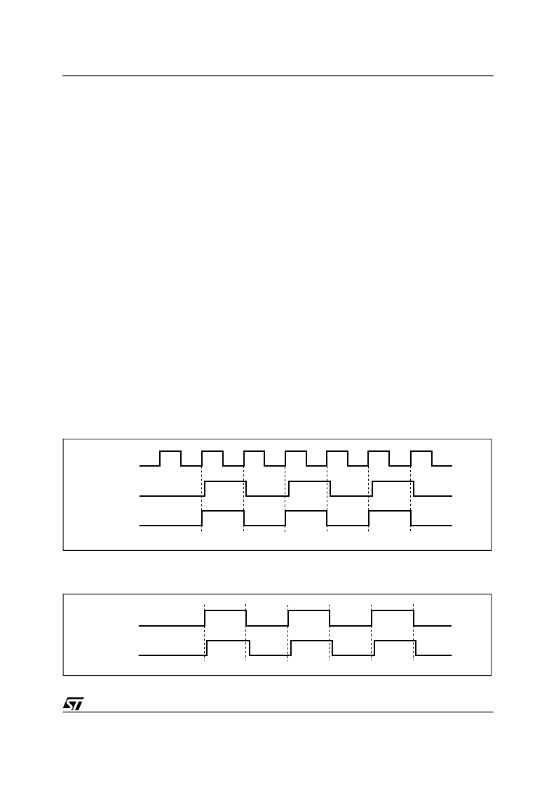
If the CLK_MODE pin is low, M7040N receives the
CLK2X and PHS_L signals. It uses the PHS_L sig-
nal to divide CLK2X and generate an internal clock
(CLK), as shown in Figure 10. The M7040N uses
CLK2X and CLK for internal operations. If the
CLK_MODE pin is high, the M7040N receives the
CLK1X only. the M7040N uses an internal PLL to
double the frequency of CLK1X and then divides
that clock by two to generate a CLK for internal op-
erations, as shown in Figure 11.
Note:
For the purpose of showing timing dia-
grams, all such diagrams in this document will be
shown in CLK2X mode. For a timing diagram in
CLK1X mode, the following substitution can be
made (see Figure 12).
Figure 10. Clocks (CLK2X and PHS_L)
Note: Any reference to
“
CLK Cycles
”
means 1 cycle of the signal,
“
CLK.
”
1.
“
CLK
”
is an internal signal.
Figure 11. Clocks (CLK1X)
1.
“
CLK
”
is an internal signal.
CLK2X
PHS_L
CLK(1)
AI04750
CLK1X
CLK(1)
AI04665
相關PDF資料 |
PDF描述 |
|---|---|
| M7040N-100ZA1T | 64K x 72-bit Entry NETWORK PACKET SEARCH ENGINE |
| M708 | PCM REMOTE CONTROL TRANSMITTER |
| M708A | PCM REMOTE CONTROL TRANSMITTER |
| M708B1 | PCM REMOTE CONTROL TRANSMITTER |
| M708AB1 | PCM REMOTE CONTROL TRANSMITTER |
相關代理商/技術參數(shù) |
參數(shù)描述 |
|---|---|
| M7040N-100ZA1T | 制造商:STMICROELECTRONICS 制造商全稱:STMicroelectronics 功能描述:64K x 72-bit Entry NETWORK PACKET SEARCH ENGINE |
| M7041 | 制造商:Tamura Corporation of America 功能描述: |
| M7045 | 制造商:Tamura Corporation of America 功能描述: |
| M705-5090142 | 功能描述:直流電源連接器 FEMALE STEREO JACK RoHS:否 制造商:Kycon 產品:Receptacles 觸點內徑: 觸點外徑: 中心腳長度: 電流額定值:7.5 A 電壓額定值:20 V 安裝角:Right 安裝風格:Cable |
| M705-5090242 | 功能描述:RCA Phono連接器 FEMALE STEREO JACK RoHS:否 制造商:Neutrik 型式:Male 端接類型:Solder 安裝風格:Cable 方向:Horizontal |
發(fā)布緊急采購,3分鐘左右您將得到回復。