- 您現(xiàn)在的位置:買賣IC網(wǎng) > PDF目錄377951 > MBM29LV320BE90TR (FUJITSU LTD) 32 M (4 M X 8/2 M X 16) BIT PDF資料下載
參數(shù)資料
| 型號(hào): | MBM29LV320BE90TR |
| 廠商: | FUJITSU LTD |
| 元件分類: | DRAM |
| 英文描述: | 32 M (4 M X 8/2 M X 16) BIT |
| 中文描述: | 2M X 16 FLASH 3V PROM, 90 ns, PDSO48 |
| 封裝: | PLASTIC, REVERSE, TSOP1-48 |
| 文件頁(yè)數(shù): | 35/64頁(yè) |
| 文件大小: | 877K |
| 代理商: | MBM29LV320BE90TR |
第1頁(yè)第2頁(yè)第3頁(yè)第4頁(yè)第5頁(yè)第6頁(yè)第7頁(yè)第8頁(yè)第9頁(yè)第10頁(yè)第11頁(yè)第12頁(yè)第13頁(yè)第14頁(yè)第15頁(yè)第16頁(yè)第17頁(yè)第18頁(yè)第19頁(yè)第20頁(yè)第21頁(yè)第22頁(yè)第23頁(yè)第24頁(yè)第25頁(yè)第26頁(yè)第27頁(yè)第28頁(yè)第29頁(yè)第30頁(yè)第31頁(yè)第32頁(yè)第33頁(yè)第34頁(yè)當(dāng)前第35頁(yè)第36頁(yè)第37頁(yè)第38頁(yè)第39頁(yè)第40頁(yè)第41頁(yè)第42頁(yè)第43頁(yè)第44頁(yè)第45頁(yè)第46頁(yè)第47頁(yè)第48頁(yè)第49頁(yè)第50頁(yè)第51頁(yè)第52頁(yè)第53頁(yè)第54頁(yè)第55頁(yè)第56頁(yè)第57頁(yè)第58頁(yè)第59頁(yè)第60頁(yè)第61頁(yè)第62頁(yè)第63頁(yè)第64頁(yè)
MBM29LV320TE/BE
80/90/10
35
I
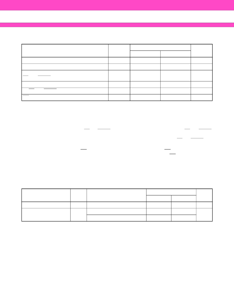
ABSOLUTE MAXIMUM RATINGS
*1 : Voltage is defined on the basis of V
SS
= GND = 0 V.
*2 : Minimum DC voltage on input or l/O pins is
0.5 V. During voltage transitions, input or I/O pins may
undershoot V
SS
to
2.0 V for periods of up to 20 ns. Maximum DC voltage on input or l/O pins is
V
CC
+
0.5 V. During voltage transitions, input or I/O pins may overshoot to V
CC
+
2.0 V for periods of up to
20 ns.
* 3: Minimum DC input voltage on A
9
, OE and RESET pins is
0.5 V. During voltage transitions, A
9
, OE and RESET
pins may undershoot V
SS
to
2.0 V for periods of up to 20 ns. Voltage difference between input
and supply voltage (V
IN
V
CC
) does not exceed
+
9.0 V.Maximum DC input voltage on A
9
, OE and RESET pins
is
+
13.0 V which may overshoot to
+
14.0 V for periods of up to 20 ns.
* 4: Minimum DC input voltage on WP/ACC pin is
0.5 V. During voltage transitions, WP/ACC pin may
undershoot V
SS
to
2.0 V for periods of up to 20 ns. Maximum DC input voltage on WP/ACC pin is
+
13.0 V which may overshoot to
+
12.0 V for periods of up to 20 ns when V
CC
is applied.
WARNING:
Semiconductor devices can be permanently damaged by application of stress (voltage, current,
temperature, etc.) in excess of absolute maximum ratings. Do not exceed these ratings.
I
RECOMMENDED OPERATING RANGES
Operating ranges define those limits between which the functionality of the device is guaranteed.
WARNING:
The recommended operating conditions are required in order to ensure the normal operation of the
semiconductor device. All of the device’s electrical characteristics are warranted when the device is
operated within these ranges.
Always use semiconductor devices within their recommended operating condition ranges. Operation
outside these ranges may adversely affect reliability and could result in device failure.
No warranty is made with respect to uses, operating conditions, or combinations not represented on
the data sheet. Users considering application outside the listed conditions are advised to contact their
FUJITSU representatives beforehand.
Parameter
Symbol
Rating
Unit
Min
55
40
Max
+
125
+
85
Storage Temperature
Tstg
°
C
°
C
Ambient Temperature with Power Applied
T
A
Voltage with Respect to Ground All pins except A
9
,
OE, and RESET *
1,
*
2
V
IN
, V
OUT
0.5
V
CC
+
0.5
V
Power Supply Voltage *
1
V
CC
0.5
0.5
0.5
+
4.0
+
13.0
+
13.0
V
A
9
, OE, and RESET *
1,
*
3
V
IN
V
WP/ACC *
1,
*
4
V
ACC
V
Parameter
Symbol
Part No.
Value
Unit
Min
40
+
3.0
+
2.7
Max
+
85
+
3.6
+
3.6
Ambient Temperature
T
A
MBM29LV320TE/BE 80/90/10
°
C
Power Supply Voltage
V
CC
MBM29LV320TE/BE 80/90
V
MBM29LV320TE/BE 10
相關(guān)PDF資料 |
PDF描述 |
|---|---|
| MBM29LV400B-12 | CMOS 4M (512K ×8/256K×16) Falsh Memory(512K ×8/256K×16位 單5V 電源電壓閃速存儲(chǔ)器) |
| MBM29LV400T-10 | CMOS 4M (512K ×8/256K×16) Falsh Memory(512K ×8/256K×16位 單5V 電源電壓閃速存儲(chǔ)器) |
| MBM29LV400T-12 | CMOS 4M (512K ×8/256K×16) Falsh Memory(512K ×8/256K×16位 單5V 電源電壓閃速存儲(chǔ)器) |
| MBM29LV400B-10 | CMOS 4M (512K ×8/256K×16) Falsh Memory(512K ×8/256K×16位 單5V 電源電壓閃速存儲(chǔ)器) |
| MBM29LV400B | CMOS 4M (512K ×8/256K×16) Falsh Memory(512K ×8/256K×16位 單5V 電源電壓閃速存儲(chǔ)器) |
相關(guān)代理商/技術(shù)參數(shù) |
參數(shù)描述 |
|---|---|
| MBM29LV320TE | 制造商:FUJITSU 制造商全稱:Fujitsu Component Limited. 功能描述:32 M (4 M X 8/2 M X 16) BIT |
| MBM29LV320TE10 | 制造商:FUJITSU 制造商全稱:Fujitsu Component Limited. 功能描述:32 M (4 M X 8/2 M X 16) BIT |
| MBM29LV320TE10PBT | 制造商:FUJITSU 制造商全稱:Fujitsu Component Limited. 功能描述:32 M (4 M X 8/2 M X 16) BIT |
| MBM29LV320TE10TN | 制造商:SPANSION 制造商全稱:SPANSION 功能描述:FLASH MEMORY |
| MBM29LV320TE10TR | 制造商:FUJITSU 制造商全稱:Fujitsu Component Limited. 功能描述:32 M (4 M X 8/2 M X 16) BIT |
發(fā)布緊急采購(gòu),3分鐘左右您將得到回復(fù)。