- 您現(xiàn)在的位置:買(mǎi)賣(mài)IC網(wǎng) > PDF目錄359169 > MK74ZD133Y PLL and 32-Output Clock Driver PDF資料下載
參數(shù)資料
| 型號(hào): | MK74ZD133Y |
| 英文描述: | PLL and 32-Output Clock Driver |
| 中文描述: | PLL和32個(gè)輸出時(shí)鐘驅(qū)動(dòng)器 |
| 文件頁(yè)數(shù): | 8/8頁(yè) |
| 文件大小: | 116K |
| 代理商: | MK74ZD133Y |
MK74ZD133
PLL and 32-Output Clock Driver
PRELIMINARY INFORMAT ION
MDS 74ZD133 C
Integrated Circuit Systems, Inc.525 Race StreetSan JoseCA95126(408)295-9800telwww.icst.com
8
Revision 010899
Printed 11/17/00
While the information presented herein has been checked for both accuracy and reliability, Integrated Circuit Systems, Inc. (ICS) assumes no responsibility for either its use or for
the infringement of any patents or other rights of third parties, which would result from its use. No other circuits, patents, or licenses are implied. This product is intended for use
in normal commercial applications. Any other applications such as those requiring extended temperature range, high reliability, or other extraordinary environmental requirements
are not recommended without additional processing by ICS. ICS reserves the right to change any circuitry or specifications without notice. ICS does not authorize or warrant any
ICS product for use in life support devices or critical medical instruments.
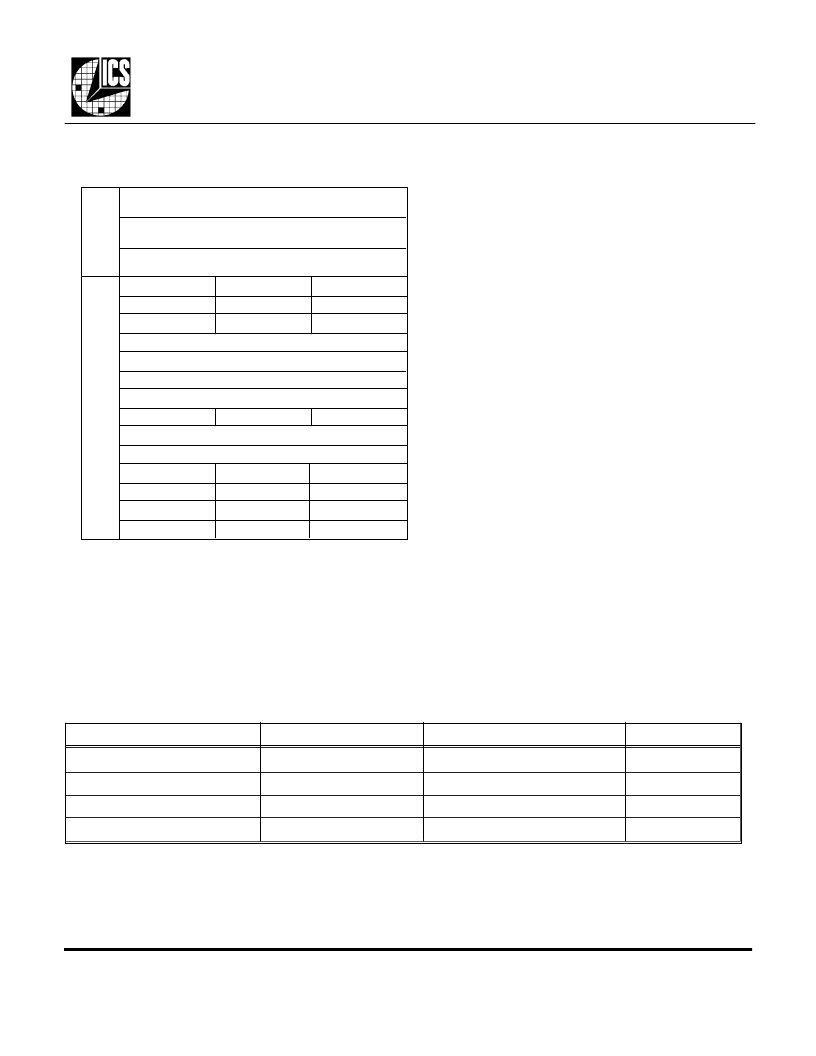
Ordering Information
Part/Order Number
MK74ZD133F
MK74ZD133FT
MK74ZD133Y
MK74ZD133YT
Marking
MK74ZD133F
MK74ZD133F
MK74ZD133Y
MK74ZD133Y
Package
Temperature
0 to 70 C
0 to 70 C
0 to 70 C
0 to 70 C
56 pin SSOP in tubes
56 SSOP in Tape & Reel
64 pin LQFP in trays
64 LQFP in Tape & Reel
Due to the large number of outputs capable
of running high speeds, the LQFP package
has an integrated heat slug to dissipate power.
When running the device above 105 MHz, or
with heavy (>15 pF) capacitive loads, it is
recommended to include a copper ground
pad, without anti-solder coating, underneath
the device. This will allow the PC board to
help in dissipating the heat created by the
MK74ZD133Y.
JEDEC VARIATION (All dimensions in millimeters)
BCD
MIN.
NOM.
MAX.
1.60
0.15
1.45
A
A1
A2
D
D1
E
E1
L
N
e
b
b1
ccc
ddd
0.05
1.35
1.40
12.00 BSC.
10.00 BSC.
12.00 BSC.
10.00 BSC.
0.60
64
0.50 BSC.
0.22
0.20
0.45
0.75
0.17
0.17
0.27
0.23
0.08
0.08
S
Y
M
B
O
L
Package Dimensions for 64 Pin LQFP
Layout Information for 64 pin LQFP
相關(guān)PDF資料 |
PDF描述 |
|---|---|
| MK74ZD133YT | PLL and 32-Output Clock Driver |
| MKW1000 | 10 Watts 2:1 Wide Input Range DC/DC Converters Single and Dual Outputs |
| MKW3024 | 20W, Wide Input Range, Single & Dual Output DC/DC Converters |
| ML2008IQ | レP Compatible Logarithmic Gain/Attenuator |
| ML2258CIP | レP Compatible 8-Bit A/D Converter with 8-Channel Multiplexer |
相關(guān)代理商/技術(shù)參數(shù) |
參數(shù)描述 |
|---|---|
| MK74ZD133YT | 制造商:ICS 制造商全稱(chēng):ICS 功能描述:PLL and 32-Output Clock Driver |
| MK75 | 制造商:Traco Power 功能描述:MOUNTING KIT TIS75 |
| MK7500F | 制造商:Ohmite Mfg Co 功能描述: |
| MK75R0F | 制造商:Ohmite Mfg Co 功能描述:Res Metal Film 75 Ohm 1% 1/4W ±50ppm/°C Conformal AXL Thru-Hole Ammo Pack |
| MK75S | 制造商:ASTRODYNE 制造商全稱(chēng):Astrodyne Corporation 功能描述:Compact 75 Watt Enclosed Switching Power Supplies |
發(fā)布緊急采購(gòu),3分鐘左右您將得到回復(fù)。