- 您現(xiàn)在的位置:買賣IC網(wǎng) > PDF目錄377972 > ML6460 (Fairchild Semiconductor Corporation) CCIR656 NTSC Video Encoder(CCIR656標(biāo)準(zhǔn)NTSC視頻編碼器) PDF資料下載
參數(shù)資料
| 型號(hào): | ML6460 |
| 廠商: | Fairchild Semiconductor Corporation |
| 英文描述: | CCIR656 NTSC Video Encoder(CCIR656標(biāo)準(zhǔn)NTSC視頻編碼器) |
| 中文描述: | CCIR656 NTSC視頻編碼器(CCIR656標(biāo)準(zhǔn)NTSC制式視頻編碼器) |
| 文件頁(yè)數(shù): | 24/30頁(yè) |
| 文件大小: | 217K |
| 代理商: | ML6460 |
第1頁(yè)第2頁(yè)第3頁(yè)第4頁(yè)第5頁(yè)第6頁(yè)第7頁(yè)第8頁(yè)第9頁(yè)第10頁(yè)第11頁(yè)第12頁(yè)第13頁(yè)第14頁(yè)第15頁(yè)第16頁(yè)第17頁(yè)第18頁(yè)第19頁(yè)第20頁(yè)第21頁(yè)第22頁(yè)第23頁(yè)當(dāng)前第24頁(yè)第25頁(yè)第26頁(yè)第27頁(yè)第28頁(yè)第29頁(yè)第30頁(yè)
ML6460
24
REV. 1.0 10/25/2000
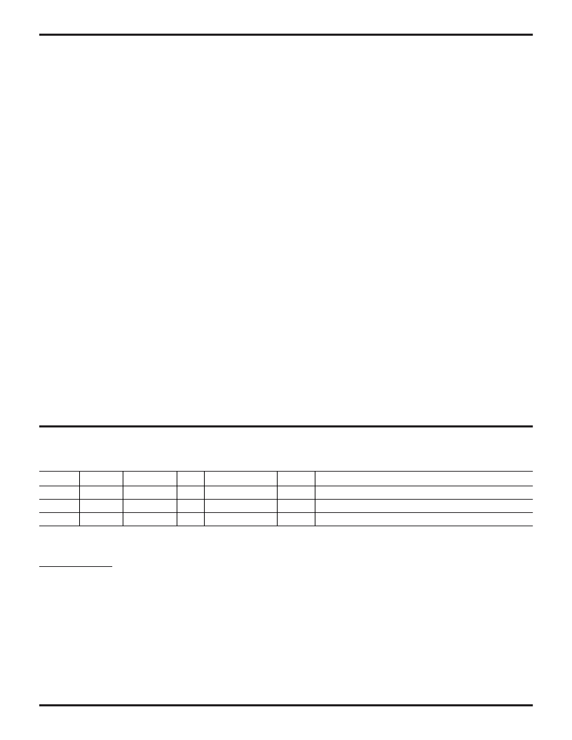
MODE PRESET1
A
B
C
D
X = don't care
* = confidential information
PRESET0
0
1
0
1
CC
XX
XX
XX
XX
CNTR
XXXXXXXX
09080209
1C080209
11080209
CPC
*
*
*
*
CPS
0
0
1
1
*
*
*
*
Mode Description
Mode A:
All register contents are programmed through serial interface.
Mode B:
Master mode, CCIR656 rate, analog blanking.
Mode C:
Slave mode, SAV and EAV codes, CCIR656 rate, digital blanking.
Mode D:
Slave mode, external sync at start of line, Square pixel rate, analog blanking
Table 8. Preset Modes and Register Values
PRESET PIN CONTROL
The ML6460 can be controlled by a pair of preset mode
pins. These pins do not allow access to all of the
programmable features of the ML6460, but are intended
to provide a simpler interface for most applications. Refer
to Table 8 for preset modes.
SERIAL BUS OPERATION
The serial bus control in the ML6460 has two levels of
addressing: Device Addressing and Functional Addressing.
Device Addressing
: Figures 15, 16, and 17 show the
physical waveforms generated in order to address the
ML6460. There are six basic parts of the waveform:
1. Start Indication: Clock Cycle 0
2. Device Address Shifted in: Clock Cycle 1 through 8
3. Device Address Strobed and Decoded: Clock Cycle 9
4. Function Address Shifted in: Clock Cycle 10 through 17
5. Function Address Strobed and Decoded: Clock Cycle 18
6. Data Shifted in 8 bits at a time, MSB first: Clock
Cycle 19 through 26
7. Data Shifted: Clock Cycle 27
8. Repeat strep 6 & 7 until all data is clocked in.
9. Stop indication: After Last Clock Cycle
(54 for CC, 54 for CNTR)
Note: data at SDATA is ignored at steps 3, 5, and 7.
Device & Function Addressing
: Figures 15, 16, an17
show the register address procedure of the ML6460.
FUNCTIONAL DESCRIPTION
(Continued)
Device Address (8 bit)
1011 0100 (Hex = B4)
Function Address (8 bit)
Closed Caption Data Registers (CC):
0000 0000
(Hex =
00)
Macrovision Control Registers (CPC): confidential
Macrovision Data Registers (CPS): confidential
Control Registers (CNTR): 0000 0011
(Hex =
03)
Number of Data Bits
Closed Caption Data Registers (CC): 4 x 8 bits
Macrovision Control Registers (CPC): confidential
Macrovision Data Registers (CPS): confidential
Control Registers (CNTR): 4 x 8 bits
CONTROL REGISTER DEFAULT SETTINGS
At Power up, the ML6460 default settings are as follows:
Control Register is undefined when the serial
bus mode is enabled.
Macrovision Register is automatically
configured by the Macrovision default
values.
Chip is ready to process video
Preset Pins are available and if used will
configure the control register.
Must write logic “0” (zero) to A30 to get
video
To get black at power up will require logic “1” in A30.
相關(guān)PDF資料 |
PDF描述 |
|---|---|
| ML6509 | Active SCSI Terminator(SCSI系統(tǒng)的有源終端器) |
| ML6510 | Series Programmable Adaptive Clock Manager(系列可編程自適應(yīng)時(shí)鐘管理器) |
| ML6516244 | 16-Bit Buffer/Line Driver with 3-State Outputs(BiCMOS 16位緩沖器/線驅(qū)動(dòng)器(三態(tài)輸出)) |
| ML6518 | 18 Line Hot-Insertable Active SCSI Terminator(線熱插入有源SCSI終端器) |
| ML65244 | High Speed Dual Quad Buffer/Line Drivers(高速雙通道四緩沖器/線驅(qū)動(dòng)器) |
相關(guān)代理商/技術(shù)參數(shù) |
參數(shù)描述 |
|---|---|
| ML6460CS | 制造商:MICRO-LINEAR 制造商全稱:MICRO-LINEAR 功能描述:NTSC Video Encoder with Macrovision |
| ML6461 | 制造商:MICRO-LINEAR 制造商全稱:MICRO-LINEAR 功能描述:NTSC Video Encoder |
| ML6461CS | 制造商:MICRO-LINEAR 制造商全稱:MICRO-LINEAR 功能描述:NTSC Video Encoder |
| ML648PTA102MLZ | 制造商:COILCRAFT 制造商全稱:Coilcraft lnc. 功能描述:High Reliability Power Inductors |
| ML64P168 | 制造商:OKI 制造商全稱:OKI electronic componets 功能描述:4-Bit Microcontroller with Built-in RC Oscillation Type A/D Converter and LCD Driver |
發(fā)布緊急采購(gòu),3分鐘左右您將得到回復(fù)。