- 您現(xiàn)在的位置:買賣IC網(wǎng) > PDF目錄45354 > MPC8245ARVV400D (FREESCALE SEMICONDUCTOR INC) 32-BIT, 400 MHz, RISC PROCESSOR, PBGA352 PDF資料下載
參數(shù)資料
| 型號: | MPC8245ARVV400D |
| 廠商: | FREESCALE SEMICONDUCTOR INC |
| 元件分類: | 微控制器/微處理器 |
| 英文描述: | 32-BIT, 400 MHz, RISC PROCESSOR, PBGA352 |
| 封裝: | 35 X 35 MM, 1.65 MM HEIGHT, 1.27 MM PITCH, LEAD FREE, TBGA-352 |
| 文件頁數(shù): | 40/68頁 |
| 文件大?。?/td> | 1143K |
| 代理商: | MPC8245ARVV400D |
第1頁第2頁第3頁第4頁第5頁第6頁第7頁第8頁第9頁第10頁第11頁第12頁第13頁第14頁第15頁第16頁第17頁第18頁第19頁第20頁第21頁第22頁第23頁第24頁第25頁第26頁第27頁第28頁第29頁第30頁第31頁第32頁第33頁第34頁第35頁第36頁第37頁第38頁第39頁當(dāng)前第40頁第41頁第42頁第43頁第44頁第45頁第46頁第47頁第48頁第49頁第50頁第51頁第52頁第53頁第54頁第55頁第56頁第57頁第58頁第59頁第60頁第61頁第62頁第63頁第64頁第65頁第66頁第67頁第68頁
MPC8245 Integrated Processor Hardware Specifications, Rev. 9
Freescale Semiconductor
45
System Design
7
System Design
This section provides electrical and thermal design recommendations for successful application of the
MPC8245.
7.1
PLL Power Supply Filtering
The AVDD and AVDD2 power signals on the MPC8245 provide power to the peripheral logic/memory bus
PLL and the MPC603e processor PLL. To ensure stability of the internal clocks, the power supplied to the
AVDD and AVDD2 input signals should be filtered of any noise in the 500-kHz to 10-MHz resonant
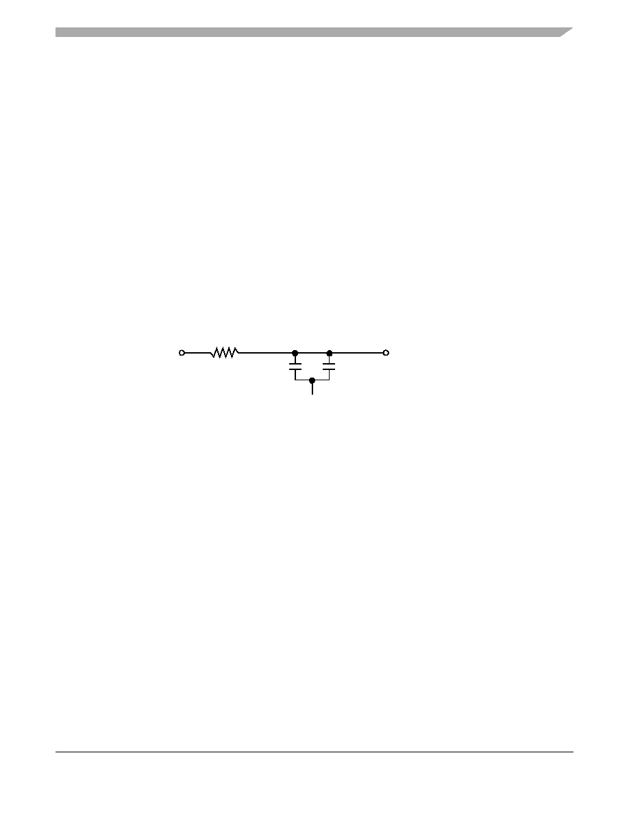
frequency range of the PLLs. Two separate circuits similar to the one shown in Figure 27 using surface
mount capacitors with minimum effective series inductance (ESL) is recommended for AVDD and AVDD2
power signal pins. Consistent with the recommendations of Dr. Howard Johnson in High Speed Digital
Design: A Handbook of Black Magic (Prentice Hall, 1993), using multiple small capacitors of equal value
is recommended over using multiple values.
Place the circuits as closely as possible to the respective input signal pins to minimize noise coupled from
nearby circuits. Routing from the capacitors to the input signal pins should be as direct as possible with
minimal inductance of vias.
Figure 27. PLL Power Supply Filter Circuit
7.2
Decoupling Recommendations
Due to its dynamic power management feature, large address and data buses, and high operating
frequencies, the MPC8245 can generate transient power surges and high frequency noise in its power
supply, especially while driving large capacitive loads. This noise must be prevented from reaching other
components in the MPC8245 system, and the MPC8245 itself requires a clean, tightly regulated source of
power. Therefore, place at least one decoupling capacitor at each VDD, OVDD, GVDD, and LVDD pin.
These decoupling capacitors should receive their power from dedicated power planes in the PCB, with
short traces to minimize inductance. These capacitors should have a value of 0.1 F. Only ceramic SMT
(surface mount technology) capacitors should be used to minimize lead inductance, preferably 0508 or
0603, oriented such that connections are made along the length of the part.
In addition, several bulk storage capacitors should be distributed around the PCB, feeding the VDD, OVDD,
GVDD, and LVDD planes, to enable quick recharging of the smaller chip capacitors. These bulk capacitors
should have a low ESR (equivalent series resistance) rating to ensure the quick response time necessary.
They should also be connected to the power and ground planes through two vias to minimize inductance.
Suggested bulk capacitors: 100–330 F (AVX TPS tantalum or Sanyo OSCON).
VDD
AVDD or AVDD2
2.2 F
GND
Low ESL Surface Mount Capacitors
10
Ω
相關(guān)PDF資料 |
PDF描述 |
|---|---|
| MPC8245TZU333D | 32-BIT, 333 MHz, RISC PROCESSOR, PBGA352 |
| MPC8245TVV350D | 32-BIT, 350 MHz, RISC PROCESSOR, PBGA352 |
| MPC8245TVV300D | 32-BIT, 300 MHz, RISC PROCESSOR, PBGA352 |
| MPC8250ACZQIHBX | 32-BIT, 200 MHz, RISC PROCESSOR, PBGA516 |
| MPC8250AVVLHDX | 32-BIT, 250 MHz, RISC PROCESSOR, PBGA480 |
相關(guān)代理商/技術(shù)參數(shù) |
參數(shù)描述 |
|---|---|
| MPC8245ARZU400D | 功能描述:微處理器 - MPU INTEGRATED HOST PROC RoHS:否 制造商:Atmel 處理器系列:SAMA5D31 核心:ARM Cortex A5 數(shù)據(jù)總線寬度:32 bit 最大時鐘頻率:536 MHz 程序存儲器大小:32 KB 數(shù)據(jù) RAM 大小:128 KB 接口類型:CAN, Ethernet, LIN, SPI,TWI, UART, USB 工作電源電壓:1.8 V to 3.3 V 最大工作溫度:+ 85 C 安裝風(fēng)格:SMD/SMT 封裝 / 箱體:FBGA-324 |
| MPC8245ARZU400D | 制造商:Freescale Semiconductor 功能描述:IC 32BIT MPU 400MHZ BGA-352 |
| MPC8245ARZU466D | 制造商:FREESCALE 制造商全稱:Freescale Semiconductor, Inc 功能描述:Part Number Specification for the MPC8245ARZUnnnX Series |
| MPC8245EC | 制造商:FREESCALE 制造商全稱:Freescale Semiconductor, Inc 功能描述:MPC8245 Integrated Processor Hardware Specifications |
| MPC8245ECS02AD | 制造商:FREESCALE 制造商全稱:Freescale Semiconductor, Inc 功能描述:MPC8245 Integrated Processor Hardware Specifications |
發(fā)布緊急采購,3分鐘左右您將得到回復(fù)。