- 您現(xiàn)在的位置:買賣IC網(wǎng) > PDF目錄25632 > MPC951FA (INTEGRATED DEVICE TECHNOLOGY INC) 951 SERIES, PLL BASED CLOCK DRIVER, 9 TRUE OUTPUT(S), 0 INVERTED OUTPUT(S), PQFP32 PDF資料下載
參數(shù)資料
| 型號(hào): | MPC951FA |
| 廠商: | INTEGRATED DEVICE TECHNOLOGY INC |
| 元件分類: | 時(shí)鐘及定時(shí) |
| 英文描述: | 951 SERIES, PLL BASED CLOCK DRIVER, 9 TRUE OUTPUT(S), 0 INVERTED OUTPUT(S), PQFP32 |
| 封裝: | 7 X 7 MM, LQFP-32 |
| 文件頁(yè)數(shù): | 6/10頁(yè) |
| 文件大小: | 336K |
| 代理商: | MPC951FA |

MPC951
TIMING SOLUTIONS
BR1333 — Rev 6
5
MOTOROLA
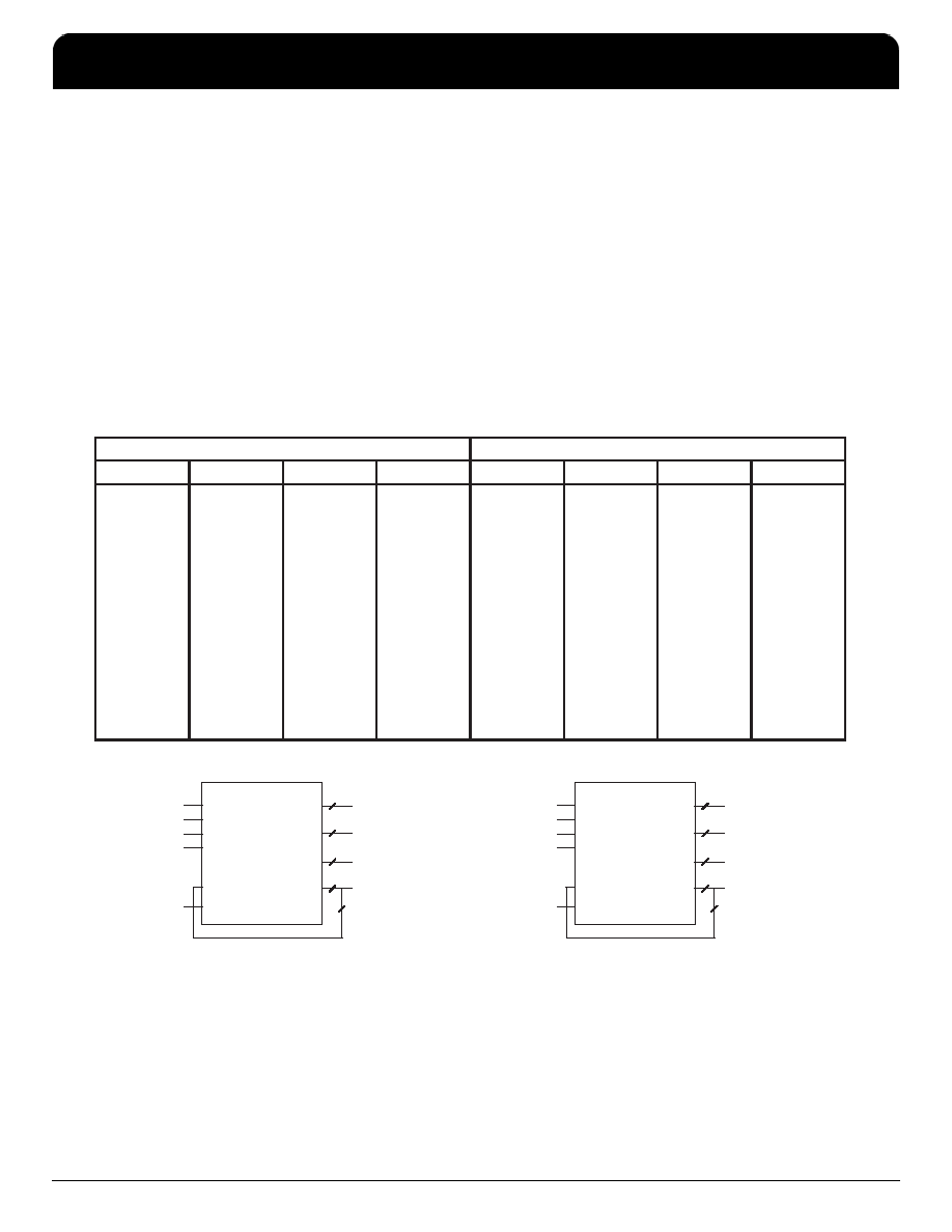
Using the MPC951 as a Zero Delay Buffer
The external feedback of the MPC951 clock driver allows
for its use as a zero delay buffer. By using one of the outputs
as a feedback to the PLL the propagation delay through the
device is eliminated. The PLL works to align the output edge
with the input reference edge thus producing a near zero
delay. The input reference frequency affects the static phase
offset of the PLL and thus the relative delay between the
inputs and outputs.
When used as a zero delay buffer the MPC951 will likely
be in a nested clock tree application. For these applications
the MPC951 offers a LVPECL clock input as a PLL reference.
This allows the user to use LVPECL as the primary clock
distribution device to take advantage of its far superior skew
performance. The MPC951 then can lock onto the LVPECL
reference and translate with near zero delay to low skew
LVCMOS outputs. Clock trees implemented in this fashion
will show significantly tighter skews than trees developed
from CMOS fanout buffers.
To minimize part–to–part skew the external feedback
option again should be used. The PLL in the MPC951
decouples the delay of the device from the propagation delay
variations of the internal gates. From the specification table
one sees a Tpd variation of only
±200ps, thus for multiple
devices under identical configurations the part–to–part skew
will be around 1000ps (350ps for Tpd variation plus 350ps
output–to–output skew plus 300ps for I/O jitter). By running
the devices at the highest possible input reference, this
part–to– part skew can be minimized. Higher input reference
frequencies will minimize both I/O jitter and tpd variations.
Table 1. Programmable Output Frequency Relationships
INPUTS
OUTPUTS
fsela
fselb
fselc
fseld
Qa
Qb
Qc
Qd
0
VCO/2
VCO/4
0
1
VCO/2
VCO/4
VCO/8
0
1
0
VCO/2
VCO/4
VCO/8
VCO/4
0
1
VCO/2
VCO/4
VCO/8
0
1
0
VCO/2
VCO/8
VCO/4
0
1
0
1
VCO/2
VCO/8
VCO/4
VCO/8
0
1
0
VCO/2
VCO/8
VCO/4
0
1
VCO/2
VCO/8
1
0
VCO/4
1
0
1
VCO/4
VCO/8
1
0
1
0
VCO/4
VCO/8
VCO/4
1
0
1
VCO/4
VCO/8
1
0
VCO/4
VCO/8
VCO/4
1
0
1
VCO/4
VCO/8
VCO/4
VCO/8
1
0
VCO/4
VCO/8
VCO/4
1
VCO/4
VCO/8
MPC951
‘1’
‘0’
Input Ref
75MHz
Ext_FB
1
MPC951
‘0’
‘1’
Input Ref
25MHz
Ext_FB
1
fsela
fselb
fselc
fseld
fsela
fselb
fselc
fseld
75MHz
Qa
75MHz
Qb
75MHz
Qc
1
2
75MHz
Qd
5
Figure 1. “Zero” Delay Buffer
Figure 2. “Zero” Delay Frequency Multiplier
1
100MHz
Qa
50MHz
Qb
50MHz
Qc
1
2
25MHz
Qd
5
Jitter Performance of the MPC951
With the clock rates of today’s digital systems continuing
to increase more emphasis is being placed on clock
distribution design and management. Among the issues
being addressed is system clock jitter and how that affects
the overall system timing budget. The MPC951 was
designed to minimize clock jitter by employing a differential
bipolar PLL as well as incorporating numerous power and
ground pins in the design. The following few paragraphs will
outline the jitter performance of the MPC951, illustrate the
measurement limitations and provide guidelines to minimize
the jitter of the device.
The most commonly specified jitter parameter is
cycle–to–cycle jitter. Unfortunately with today’s high
performance measurement equipment there is no way to
measure this parameter for jitter performance in the class
demonstrated by the MPC951. As a result different methods
are used which approximate cycle–to–cycle jitter. The typical
method of measuring the jitter is to accumulate a large
number of cycles, create a histogram of the edge placements
MPC951
Low Voltage PLL Clock Driver
NETCOM
IDT Low Voltage PLL Clock Driver
Freescale Timing Solutions Organization has been acquired by Integrated Device Technology, Inc
MPC951
5
相關(guān)PDF資料 |
PDF描述 |
|---|---|
| MPC961CFA | 961 SERIES, PLL BASED CLOCK DRIVER, 17 TRUE OUTPUT(S), 0 INVERTED OUTPUT(S), PQFP32 |
| MPC962304D-1R2 | 962304 SERIES, PLL BASED CLOCK DRIVER, 4 TRUE OUTPUT(S), 0 INVERTED OUTPUT(S), PDSO8 |
| MPC96877EP | PLL BASED CLOCK DRIVER, 10 TRUE OUTPUT(S), 0 INVERTED OUTPUT(S), QCC40 |
| MPC97R73FA | PLL BASED CLOCK DRIVER, 12 TRUE OUTPUT(S), 0 INVERTED OUTPUT(S), PQFP52 |
| MPC9892FA | PLL BASED CLOCK DRIVER, 5 TRUE OUTPUT(S), 0 INVERTED OUTPUT(S), PQFP32 |
相關(guān)代理商/技術(shù)參數(shù) |
參數(shù)描述 |
|---|---|
| MPC951FAR2 | 制造商:Motorola Inc 功能描述: |
| MPC952 | 制造商:MOTOROLA 制造商全稱:Motorola, Inc 功能描述:LOW VOLTAGE PLL CLOCK DRIVER |
| MPC953 | 制造商:MOTOROLA 制造商全稱:Motorola, Inc 功能描述:LOW VOLTAGE PLL CLOCK DRIVER |
| MPC958 | 制造商:MOTOROLA 制造商全稱:Motorola, Inc 功能描述:LOW VOLTAGE PLL CLOCK DRIVER |
| MPC9600 | 制造商:MOTOROLA 制造商全稱:Motorola, Inc 功能描述:LOW VOLTAGE 2.5 V AND 3.3 V CMOS PLL CLOCK DRIVER |
發(fā)布緊急采購(gòu),3分鐘左右您將得到回復(fù)。