- 您現(xiàn)在的位置:買賣IC網(wǎng) > PDF目錄224505 > MT46V32M16BN-5BLIT 32M X 16 DDR DRAM, 0.7 ns, PBGA60 PDF資料下載
參數(shù)資料
| 型號: | MT46V32M16BN-5BLIT |
| 元件分類: | DRAM |
| 英文描述: | 32M X 16 DDR DRAM, 0.7 ns, PBGA60 |
| 封裝: | 10 X 12.50 MM, LEAD FREE, PLASTIC, FBGA-60 |
| 文件頁數(shù): | 35/82頁 |
| 文件大小: | 2855K |
| 代理商: | MT46V32M16BN-5BLIT |
第1頁第2頁第3頁第4頁第5頁第6頁第7頁第8頁第9頁第10頁第11頁第12頁第13頁第14頁第15頁第16頁第17頁第18頁第19頁第20頁第21頁第22頁第23頁第24頁第25頁第26頁第27頁第28頁第29頁第30頁第31頁第32頁第33頁第34頁當前第35頁第36頁第37頁第38頁第39頁第40頁第41頁第42頁第43頁第44頁第45頁第46頁第47頁第48頁第49頁第50頁第51頁第52頁第53頁第54頁第55頁第56頁第57頁第58頁第59頁第60頁第61頁第62頁第63頁第64頁第65頁第66頁第67頁第68頁第69頁第70頁第71頁第72頁第73頁第74頁第75頁第76頁第77頁第78頁第79頁第80頁第81頁第82頁
512Mb: x4, x8, x16
DDR SDRAM
09005aef80a1d9e7
Micron Technology, Inc., reserves the right to change products or specifications without notice.
512MBDDRx4x8x16_2.fm - Rev. H 7/04 EN
40
2000 Micron Technology, Inc. All rights reserved.
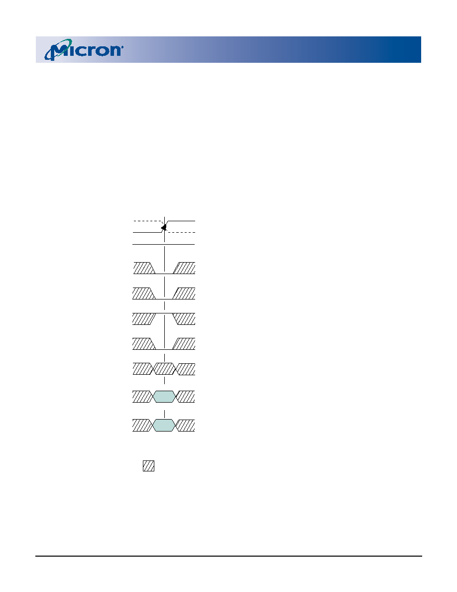
PRECHARGE
The PRECHARGE command (Figure 31) is used to
deactivate the open row in a particular bank or the
open row in all banks. The bank(s) will be available for
a subsequent row access some specified time (tRP)
after the PRECHARGE command is issued. Input A10
determines whether one or all banks are to be pre-
charged, and in the case where only one bank is to be
precharged, inputs BA0, BA1 select the bank. When all
banks are to be precharged, inputs BA0, BA1 are
treated as “Don’t Care.” Once a bank has been pre-
charged, it is in the idle state and must be activated
prior to any READ or WRITE commands being issued
to that bank.
Figure 31: PRECHARGE Command
Power-down (CKE Not Active)
Unlike SDR SDRAMs, DDR SDRAMs require CKE to
be active at all times an access is in progress, from the
issuing of a READ or WRITE command until comple-
tion of the access. Thus a clock suspend is not sup-
ported. For READs, an access completion is defined
when the Read Postamble is satisfied; for WRITEs, an
access completion is defined when the Write Recovery
time (tWR) is satisfied.
Power-down as shown in Figure 32 on page 41, is
entered when CKE is registered LOW and all Table 7
(page 41) criteria are met. If power-down occurs when
all banks are idle, this mode is referred to as precharge
power-down; if power-down occurs when there is a
row active in any bank, this mode is referred to as
active power-down. Entering power-down deactivates
the input and output buffers, excluding CK, CK#, and
CKE. For maximum power savings, the DLL is frozen
during precharge power-down mode. Exiting power-
down requires the device to be at the same voltage and
frequency as when it entered power-down. However,
power-down duration is limited by the refresh require-
ments of the device (tREFC).
While in power-down, CKE LOW and a stable clock
signal must be maintained at the inputs of the DDR
SDRAM, while all other input signals are “Don’t Care.”
The power-down state is synchronously exited when
CKE is registered HIGH (in conjunction with a NOP or
DESELECT command). A valid executable command
may be applied one clock cycle later.
CS#
WE#
CAS#
RAS#
CKE
A10
BA0,1
HIGH
ALL BANKS
ONE BANK
BA
A0–A9, A11, A12
CK
CK#
BA = Bank Address (if A10 is LOW;
otherwise “Don’t Care”)
DON’T CARE
相關(guān)PDF資料 |
PDF描述 |
|---|---|
| MT46V32M81AZ4-6T:G | 32M X 4 DDR DRAM, 0.75 ns, PDSO66 |
| MT47H128M8HV-187ELIT:E | 128M X 8 DDR DRAM, 0.35 ns, PBGA60 |
| MT47H128M8HQ-187ELAT:E | 128M X 8 DDR DRAM, 0.35 ns, PBGA60 |
| MT48LC2M32B1TG-7 | 2M X 32 SYNCHRONOUS DRAM, 5.5 ns, PDSO86 |
| MT48LC32M4A2P-7ELIT:G | 32M X 4 SYNCHRONOUS DRAM, 5.4 ns, PDSO54 |
相關(guān)代理商/技術(shù)參數(shù) |
參數(shù)描述 |
|---|
發(fā)布緊急采購,3分鐘左右您將得到回復。