- 您現(xiàn)在的位置:買賣IC網(wǎng) > PDF目錄224505 > MT46V32M16BN-5BLIT 32M X 16 DDR DRAM, 0.7 ns, PBGA60 PDF資料下載
參數(shù)資料
| 型號(hào): | MT46V32M16BN-5BLIT |
| 元件分類: | DRAM |
| 英文描述: | 32M X 16 DDR DRAM, 0.7 ns, PBGA60 |
| 封裝: | 10 X 12.50 MM, LEAD FREE, PLASTIC, FBGA-60 |
| 文件頁數(shù): | 77/82頁 |
| 文件大?。?/td> | 2855K |
| 代理商: | MT46V32M16BN-5BLIT |
第1頁第2頁第3頁第4頁第5頁第6頁第7頁第8頁第9頁第10頁第11頁第12頁第13頁第14頁第15頁第16頁第17頁第18頁第19頁第20頁第21頁第22頁第23頁第24頁第25頁第26頁第27頁第28頁第29頁第30頁第31頁第32頁第33頁第34頁第35頁第36頁第37頁第38頁第39頁第40頁第41頁第42頁第43頁第44頁第45頁第46頁第47頁第48頁第49頁第50頁第51頁第52頁第53頁第54頁第55頁第56頁第57頁第58頁第59頁第60頁第61頁第62頁第63頁第64頁第65頁第66頁第67頁第68頁第69頁第70頁第71頁第72頁第73頁第74頁第75頁第76頁當(dāng)前第77頁第78頁第79頁第80頁第81頁第82頁
512Mb: x4, x8, x16
DDR SDRAM
09005aef80a1d9e7
Micron Technology, Inc., reserves the right to change products or specifications without notice.
512MBDDRx4x8x16_2.fm - Rev. H 7/04 EN
79
2000 Micron Technology, Inc. All rights reserved.
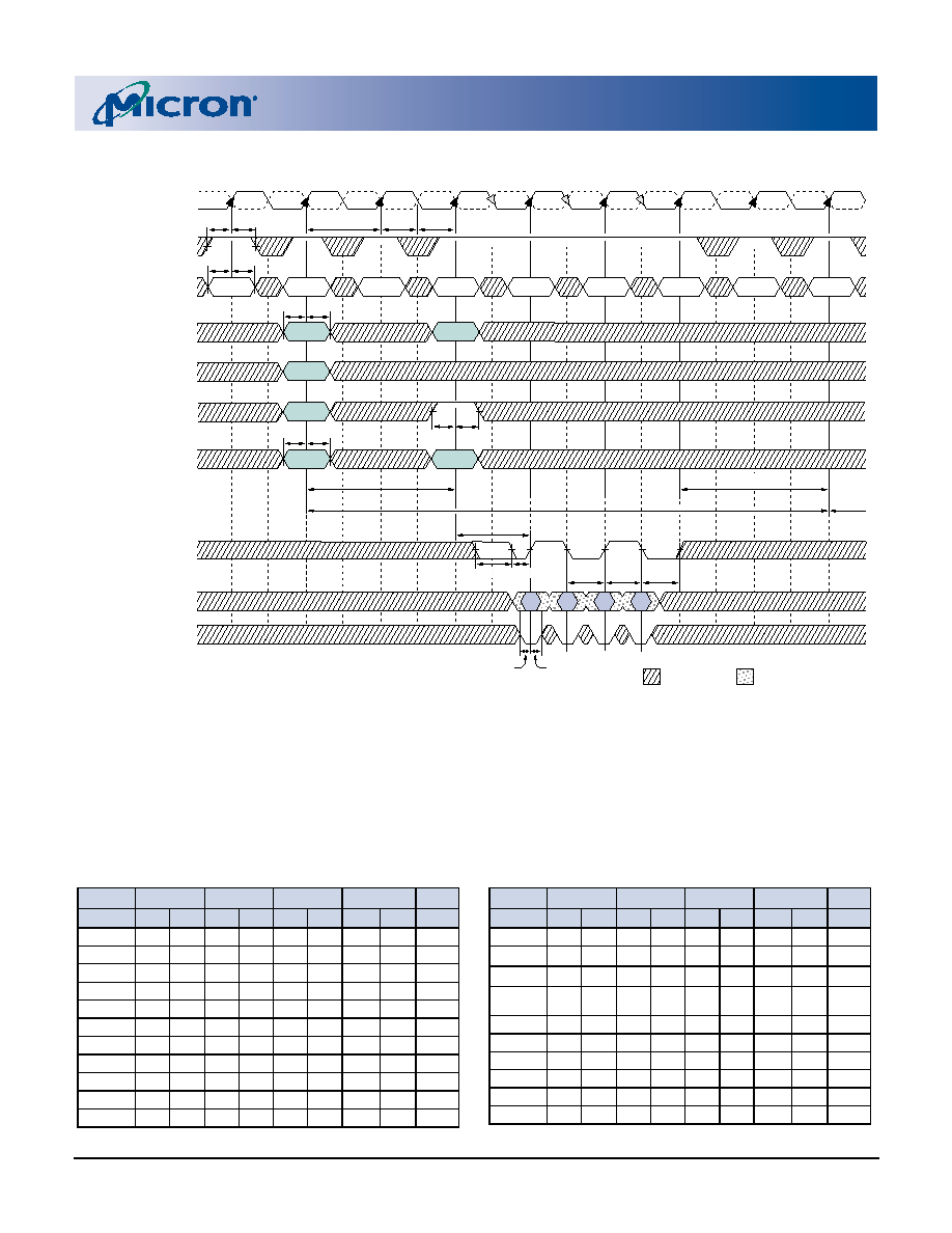
Figure 52: Bank Write - With Auto Precharge
NOTE:
1. DIn = data-out from column n; subsequent elements are provided in the programmed order.
2. Burst length = 4 in the case shown.
3. Enable auto precharge.
4. ACT = ACTIVE, RA = Row Address, BA = Bank Address.
5. NOP commands are shown for ease of illustration; other commands may be valid at these times.
6. See Figure 43, ”Data Input Timing” on page 70 for detailed DQ timing.
CK
CK#
CKE
A10
BA0, BA1
tCK
tCH
tCL
tIS
tIH
tIS
tIH
tIS
tIH
RA
tRCD
tRAS
tRP
tWR
T0
T1
T2
T3
T4
T5
T5n
T6
T7
T8
T4n
NOP5
COMMAND4
3
ACT
RA
Col n
WRITE2
NOP5
Bank x
NOP5
Bank x
NOP5
tDQSL tDQSH tWPST
DQ1
DQS
DM
DI
b
tDS
tDH
tDQSS (NOM)
DON’T CARE
TRANSITIONING DATA
tWPRES tWPRE
x8: A12
x16: A11, A12
x4: A0–A9, A11, A12
x8: A0–A9, A11
x16: A0–A9
-5B
-6/-6T
-75E/75Z
-75
SYMBOL MIN MAX MIN MAX MIN MAX MIN MAX UNITS
tCH
0.45 0.55 0.45 0.55 0.45 0.55
0.45
0.55
tCK
tCL
0.45 0.55 0.45 0.55 0.45 0.55
0.45
0.55
tCK
tCK (3)
5
7,5
NA
ns
tCK (2.5)
6
13
6
13
7.5
13
7.5
13
ns
tCK (2)
7.5
13
7.5
13
7.5
13
10
13
ns
tDH
0.45
0.5
ns
tDS
0.45
ns
tDQSH 0.35
0.35
tCK
tDQSL
0.35
tCK
tDQSS
0.72 1.28 0.75 1.25 0.75 1.25
0.75
1.25
tCK
tDSS
0.2
tCK
tDSH
0.2
tCK
tIH
S
0.75
0.8
1
ns
tIS
S
0.75
0.8
1
ns
tRAS
40
70,00
0
42
70,00
0
40
120,00
0
40
120,00
0
ns
tRCD
15
20
ns
tRP
15
20
ns
tWPRE 0.25
0.25
tCK
tWPRES
00
0
ns
tWPST
0.4
0.6
0.4
0.6
0.4
0.6
tCK
tWR
15
ns
-5B
-6/-6T
-75E/75Z
-75
SYMBOL MIN MAX MIN MAX MIN MAX MIN MAX UNITS
相關(guān)PDF資料 |
PDF描述 |
|---|---|
| MT46V32M81AZ4-6T:G | 32M X 4 DDR DRAM, 0.75 ns, PDSO66 |
| MT47H128M8HV-187ELIT:E | 128M X 8 DDR DRAM, 0.35 ns, PBGA60 |
| MT47H128M8HQ-187ELAT:E | 128M X 8 DDR DRAM, 0.35 ns, PBGA60 |
| MT48LC2M32B1TG-7 | 2M X 32 SYNCHRONOUS DRAM, 5.5 ns, PDSO86 |
| MT48LC32M4A2P-7ELIT:G | 32M X 4 SYNCHRONOUS DRAM, 5.4 ns, PDSO54 |
相關(guān)代理商/技術(shù)參數(shù) |
參數(shù)描述 |
|---|
發(fā)布緊急采購,3分鐘左右您將得到回復(fù)。