- 您現(xiàn)在的位置:買賣IC網(wǎng) > PDF目錄385639 > MT46V64M8 (Micron Technology, Inc.) 16 Meg x 8 x 4 banks DDR SDRAM(16M x 8 x 4組,雙數(shù)據(jù)速率同步動態(tài)RAM) PDF資料下載
參數(shù)資料
| 型號: | MT46V64M8 |
| 廠商: | Micron Technology, Inc. |
| 英文描述: | 16 Meg x 8 x 4 banks DDR SDRAM(16M x 8 x 4組,雙數(shù)據(jù)速率同步動態(tài)RAM) |
| 中文描述: | 16梅格× 8 × 4銀行DDR SDRAM內(nèi)存(1,600 × 8 × 4組,雙數(shù)據(jù)速率同步動態(tài)RAM)的 |
| 文件頁數(shù): | 64/70頁 |
| 文件大?。?/td> | 2524K |
| 代理商: | MT46V64M8 |
第1頁第2頁第3頁第4頁第5頁第6頁第7頁第8頁第9頁第10頁第11頁第12頁第13頁第14頁第15頁第16頁第17頁第18頁第19頁第20頁第21頁第22頁第23頁第24頁第25頁第26頁第27頁第28頁第29頁第30頁第31頁第32頁第33頁第34頁第35頁第36頁第37頁第38頁第39頁第40頁第41頁第42頁第43頁第44頁第45頁第46頁第47頁第48頁第49頁第50頁第51頁第52頁第53頁第54頁第55頁第56頁第57頁第58頁第59頁第60頁第61頁第62頁第63頁當(dāng)前第64頁第65頁第66頁第67頁第68頁第69頁第70頁
64
512Mb: x4, x8, x16 DDR SDRAM
512Mx4x8x16DDR_A.p65
–
Rev. A; Pub 10/00
Micron Technology, Inc., reserves the right to change products or specifications without notice.
2000, Micron Technology, Inc.
512Mb: x4, x8, x16
DDR SDRAM
ADVANCE
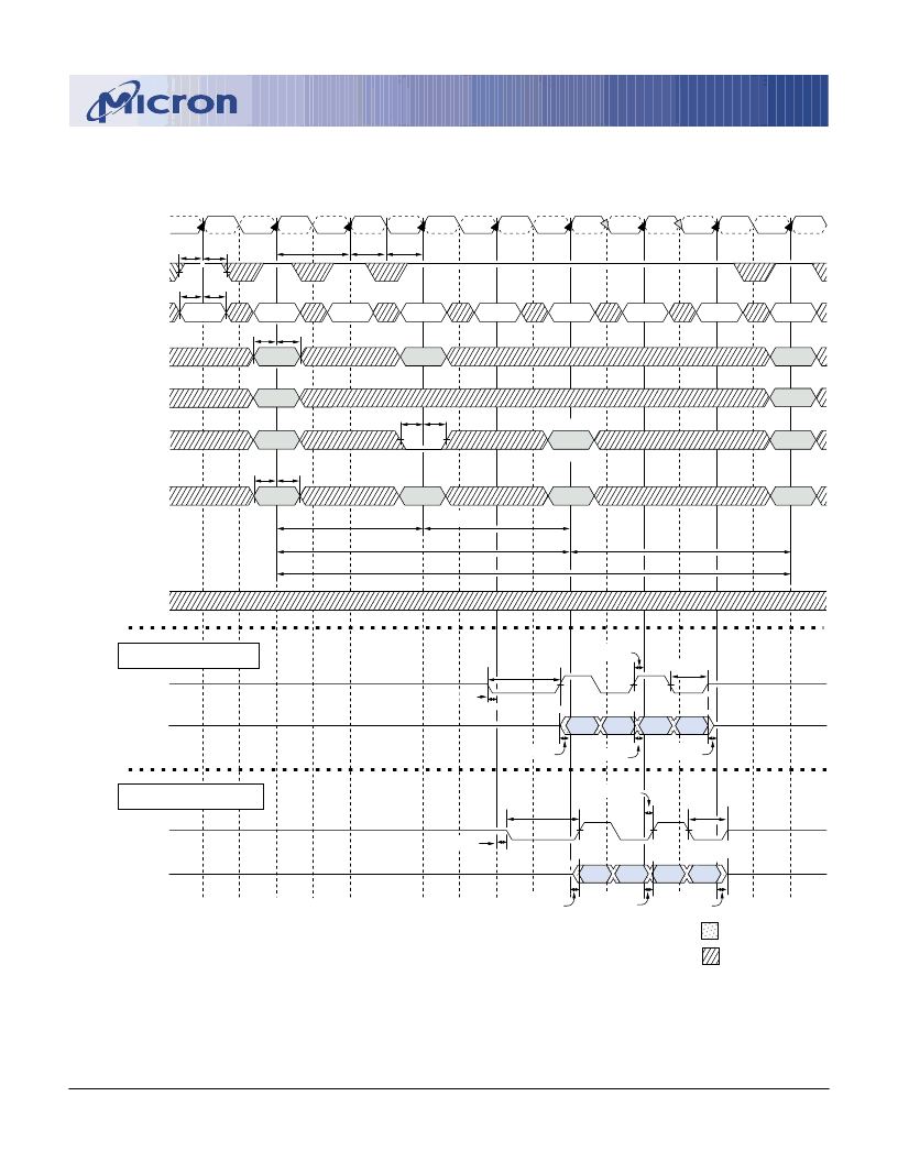
BANK READ – WITHOUT AUTO PRECHARGE
CK
CK#
CKE
A10
BA0, BA1
t
CK
t
CH
t
CL
t
IS
t
IS
t
IH
t
IS
t
IS
t
IH
t
IH
t
IH
t
IS
t
IH
RA
t
RCD
t
RAS7
t
RC
t
RP
CL = 2
DM
T0
T1
T2
T3
T4
T5
T5n
T6n
T6
T7
T8
DQ
1
DQS
Case 1:
t
AC
(
MIN)
and
t
DQSCK
(
MIN)
Case 2:
t
AC
(
MAX)
and
t
DQSCK
(
MAX)
DQ
1
DQS
t
RPRE
t
RPRE
t
RPST
t
RPST
t
DQSCK
(
MIN)
t
DQSCK
(
MAX)
t
LZ
(
MIN)
t
LZ
(
MAX)
t
AC
(
MIN)
t
LZ
(
MIN)
DO
n
t
HZ
(
MAX)
t
AC
(
MAX)
t
LZ
(
MAX)
DO
n
NOP6
NOP6
COMMAND
5
3
ACT
RA
RA
Col
n
READ2
PRE
7
Bank
x
RA
RA
RA
Bank
x
Bank
x
4
ACT
Bank
x
NOP6
NOP6
NOP6
t
HZ
(
MIN)
NOTE:
1. DO
n
= data-out from column
n
; subsequent elements are provided in the programmed order.
2. Burst length = 4 in the case shown.
3. Disable auto precharge.
4.
“
Don
’
t Care
”
if A10 is HIGH at T5.
5. PRE = PRECHARGE, ACT = ACTIVE, RA = Row Address, BA = Bank Address.
6. NOP commands are shown for ease of illustration; other commands may be valid at these times.
7. The PRECHARGE command can only be applied at T5 if
t
RAS minimum is met.
8. Refer to figure 27, 27A, and 28 for detailed DQS and DQ timing.
ONE BANK
ALL BANKS
DON
’
T CARE
TRANSITIONING DATA
x4: A0-A9, A11, A12
x8: A0-A11
x16: A0-A9
x8: A12
x16: A11, A12
相關(guān)PDF資料 |
PDF描述 |
|---|---|
| MT48LC16M8A1TG | SYNCHRONOUS DRAM |
| MT48LC32M4A1 | ECONOLINE: RSZ/P - 1kVDC |
| MT48LC32M4A2 | SYNCHRONOUS DRAM |
| MT48LC32M4A1TG | SYNCHRONOUS DRAM |
| MT48LC8M16A1TG | SYNCHRONOUS DRAM |
相關(guān)代理商/技術(shù)參數(shù) |
參數(shù)描述 |
|---|
發(fā)布緊急采購,3分鐘左右您將得到回復(fù)。