- 您現(xiàn)在的位置:買賣IC網(wǎng) > PDF目錄373275 > RK80530KZ006512 MICROPROCESSOR|32-BIT|CMOS|PGA|370PIN|CERAMIC PDF資料下載
參數(shù)資料
| 型號(hào): | RK80530KZ006512 |
| 英文描述: | MICROPROCESSOR|32-BIT|CMOS|PGA|370PIN|CERAMIC |
| 中文描述: | 微處理器| 32位|的CMOS |美巡賽| 370PIN |陶瓷 |
| 文件頁數(shù): | 29/86頁 |
| 文件大小: | 882K |
| 代理商: | RK80530KZ006512 |
第1頁第2頁第3頁第4頁第5頁第6頁第7頁第8頁第9頁第10頁第11頁第12頁第13頁第14頁第15頁第16頁第17頁第18頁第19頁第20頁第21頁第22頁第23頁第24頁第25頁第26頁第27頁第28頁當(dāng)前第29頁第30頁第31頁第32頁第33頁第34頁第35頁第36頁第37頁第38頁第39頁第40頁第41頁第42頁第43頁第44頁第45頁第46頁第47頁第48頁第49頁第50頁第51頁第52頁第53頁第54頁第55頁第56頁第57頁第58頁第59頁第60頁第61頁第62頁第63頁第64頁第65頁第66頁第67頁第68頁第69頁第70頁第71頁第72頁第73頁第74頁第75頁第76頁第77頁第78頁第79頁第80頁第81頁第82頁第83頁第84頁第85頁第86頁
Datasheet
29
Intel
Pentium
III Processor with 512KB L2 Cache at 1.13GHz to 1.40GHz
2.11
AGTL System Bus Specifications
It is recommended that the AGTL bus be routed in a daisy-chain fashion with termination resistors
to V
TT
. These termination resistors are placed electrically between the ends of the signal traces and
the V
TT
voltage supply. The valid high and low levels are determined by the input buffers using a
reference voltage called V
REF
. Refer to the appropriate platform design guide for more information
Table 13
below lists the nominal specification for the AGTL termination voltage (V
TT
). The AGTL
reference voltage (V
REF
) is generated on the system motherboard and should be set to 2/3 V
TT
for
the processor and other AGTL logic. It is important that the baseboard impedance be specified and
held to a ±15% tolerance, and that the intrinsic trace capacitance for the AGTL signal group traces
is known and well-controlled. For more details on the AGTL buffer specification, see the
Intel
Pentium
II Processor Developer's Manual
and AP-585,
Intel
Pentium
II Processor
AGTL Guidelines
.
NOTES:
1. Unless otherwise noted, all specifications in this table apply to Intel Pentium III processors with 512KB L2
cache at all frequencies.
2. Intel Pentium III processors with 512KB L2 cache for the PGA370 socket contain AGTL termination
resistors on the processor die, except for the RESET# input.
3. V
TT
must be held to 1.25V ±9%. It is required that V
TT
be held to 1.25V ±3% while the processor system bus
is idle (static condition). This is measured at the PGA370 socket pins on the bottom side of the baseboard.
4. Uni-processor platforms require a 56
resistor and dual-processor platforms require a 68
resistor.
Tolerance for on-die Rtt is +/-10% (56, 68
resistors). Rtt is +/-15% (100
resistors).
5. V
REF
is generated on the motherboard and should be 2/3 V
TT
±5% nominally. Ensure that there is adequate
V
REF
decoupling on the motherboard.
2.12
System Bus Timing Specifications
The processor system bus timings specified in this section are defined at the socket pins on the
bottom of the motherboard. Unless otherwise specified, timings are tested at the processor pins
during manufacturing. Timings at the processor pins are specified by design characterization. See
Section 7.0
for the processor signal definitions.
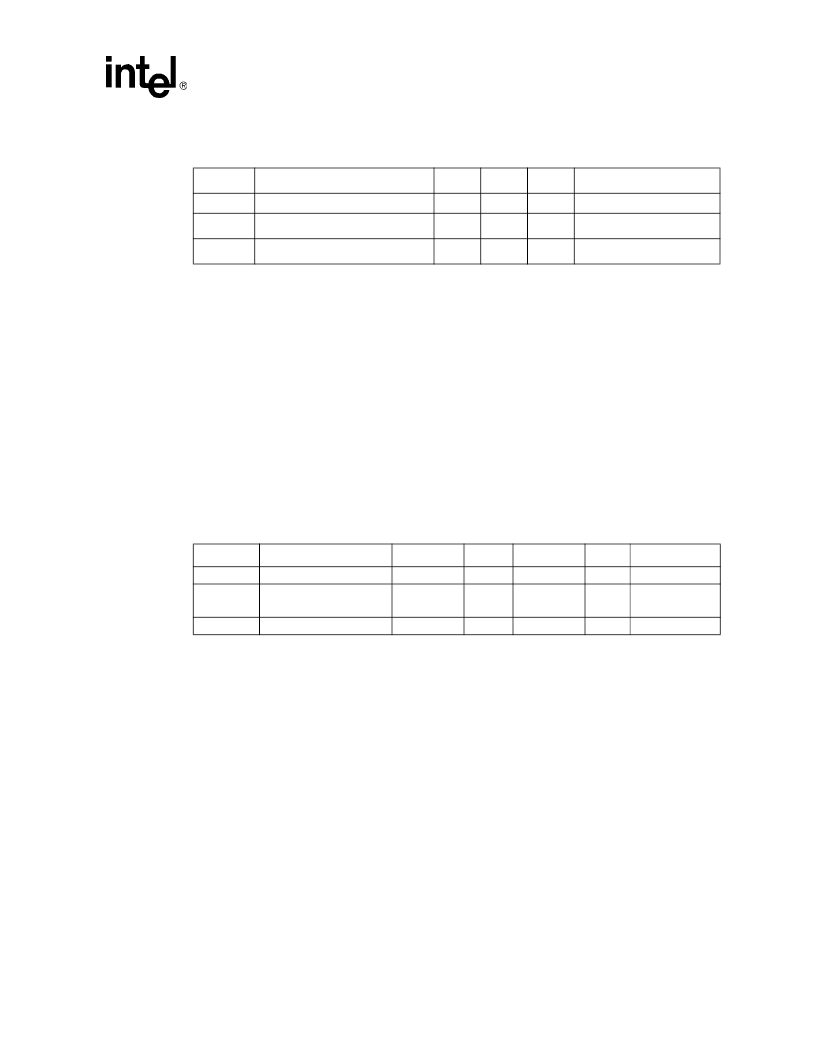
Table 12. 3.3 Volt CMOS Output Signal Group DC Specifications
Symbol
Parameter
Min
Max
Unit
Notes
V
Nominal Voltage
3.45
V
3.3 + 5%
V
OH
Output High Voltage
0.9
V
I
LO
Output Leakage Current
100
μA
Table 13. Processor AGTL Bus Specifications
1, 2
Symbol
Parameter
Min
Typ
Max
Units
Notes
V
TT
Bus Termination Voltage
1.1375
1.25
56
68
2/3V
TT
V
3
On-die R
TT
Termination Resistor
50
115
4
V
REF
Bus Reference Voltage
V
5
相關(guān)PDF資料 |
PDF描述 |
|---|---|
| RK80530KZ012512 | Metal Film Resistor - RN 1/4 T1 110 1% A |
| RK80530KZ017512 | MICROPROCESSOR|32-BIT|CMOS|PGA|370PIN|CERAMIC |
| RK80532PC041512 | Microprocessor |
| RK9410 | TRANSISTOR | MOSFET | N-CHANNEL | 30V V(BR)DSS | 7A I(D) | SO |
| RKC-SERIES | Interface IC |
相關(guān)代理商/技術(shù)參數(shù) |
參數(shù)描述 |
|---|---|
| RK80530KZ012512 | 制造商:Intel 功能描述:MPU Pentium 制造商:Rochester Electronics LLC 功能描述:P3 (TUALATIN) 1.26GHZ 512 CACHE (FOR SERVERS) 133 FSB; 1.45V - Bulk |
| RK80530KZ012512S L5QL | 制造商:Intel 功能描述:MPU Pentium 制造商:Intel 功能描述:MPU Pentium? III Processor-S 64-Bit 0.13um 1.26GHz 370-Pin FCPGA2 |
| RK80530KZ012512S L6BX | 制造商:Intel 功能描述:MPU Pentium 制造商:Intel 功能描述:MPU Pentium? III Processor-S 64-Bit 0.13um 1.26GHz 370-Pin FCPGA 制造商:Intel 功能描述:MPU PENTIUM III 64BIT 0.13UM 1.266GHZ 370PIN FCPGA2 - Trays |
| RK80530KZ017512 | 制造商:Rochester Electronics LLC 功能描述:P3 (TUALATIN) 1.4HZ 512 CACHE (FOR SERVERS) 133 FSB; 1.45V - Bulk |
| RK80530KZ017512S L5XL | 制造商:Intel 功能描述:32BIT MPU 80530KZ017512 1.40G |
發(fā)布緊急采購,3分鐘左右您將得到回復(fù)。