- 您現(xiàn)在的位置:買(mǎi)賣(mài)IC網(wǎng) > PDF目錄373348 > S39421S (Electronic Theatre Controls, Inc.) Hot Swap Voltage Controller PDF資料下載
參數(shù)資料
| 型號(hào): | S39421S |
| 廠(chǎng)商: | Electronic Theatre Controls, Inc. |
| 英文描述: | Hot Swap Voltage Controller |
| 中文描述: | 電壓熱插拔控制器 |
| 文件頁(yè)數(shù): | 13/28頁(yè) |
| 文件大小: | 201K |
| 代理商: | S39421S |
第1頁(yè)第2頁(yè)第3頁(yè)第4頁(yè)第5頁(yè)第6頁(yè)第7頁(yè)第8頁(yè)第9頁(yè)第10頁(yè)第11頁(yè)第12頁(yè)當(dāng)前第13頁(yè)第14頁(yè)第15頁(yè)第16頁(yè)第17頁(yè)第18頁(yè)第19頁(yè)第20頁(yè)第21頁(yè)第22頁(yè)第23頁(yè)第24頁(yè)第25頁(yè)第26頁(yè)第27頁(yè)第28頁(yè)
S39421
13
2024 9.0 8/8/00
INSTRUCTION SET
Instruction
Start
Bit
Opcode
Address
x16
Data
x16
Comments
READ
1
10
x(A5
–
A0)
Read Address AN
–
A0
ERASE
1
11
x(A5
–
A0)
Clear Address AN
–
A0
WRITE
1
01
x(A5
–
A0)
D15
–
D0
Write Address AN
–
A0
EWEN
1
00
11xxxx
Write Enable
EWDS
1
00
00xxxx
Write Disable
WRAL
1
00
01xxxx
D15
–
D0
Write All Addresses
2024 PGM T5 .0
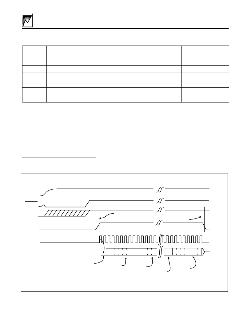
FIGURE 11. DATA DOWNLOADER SEQUENCE OF OPERATION
[note: all data download timing conforms to the timing shown in Figure 5]
Data Download Mode
The Data Download mode is an alternative method of
accessing the E
2
PROM memory. Use of this mode allows
downloading the entire contents of the memory without
entering any commands. The DD mode is enabled after a
low to high transition on the DD pin, while continuing to
assert DD (this includes powering up the device with DD
tied high). Also, as a condition to enter this mode, the
device must not be in a state of reset. Once in Data
Download mode, the device will wait until Chip Select is
driven active. At this point, the device will output a dummy
‘
0
’
followed by the contents of location 0000. As long as
the SK line is toggled the S39421 will continue to output
the contents of sequential address locations. In this
manner, the configuration data that is loaded into an
interface device can be accessed in a simple manner
without requiring the logic of the interface chip to generate
the complex signals needed for the microwire interface.
Data Download mode is exited upon the first high to low
transition of the Chip Select input.
Data From
Address 000
Data From
Address 001 Data From
Address 1FE
Data From
Address 1FF
DO
SK
CS
DD
VCC
Dummy 0
2024 ILL7.1
DD Mode
Disabled
DD Mode Enabled After
RESET is released and After
DD is Taken to Logic 1
RESET
相關(guān)PDF資料 |
PDF描述 |
|---|---|
| S3954 | 76-element Si photodiode array High UV sensitivity photodiode array mounted in DIP |
| S3994-01 | Si PIN photodiode for optical power meters |
| S3AB | 3.0A SURFACE MOUNT GLASS PASSVATED RECTIFIER |
| S3MB | 3.0A FAST RECOVERY GLASS PASSIVATED RECTIFIER |
| S3KB | 3.0A FAST RECOVERY GLASS PASSIVATED RECTIFIER |
相關(guān)代理商/技術(shù)參數(shù) |
參數(shù)描述 |
|---|---|
| S394-90-108-00-760000 | 制造商:Mill-Max Mfg Corp 功能描述:Custom Socket |
| S3950G2NR | 制造商:TYAN 功能描述:1P/AMD,(2)LAN,PCI-X,(4)PCI,ATX - Trays |
| S3950G2NR RPL | 制造商:TYAN 功能描述:REPAIR/REPLACEMENT - Bulk |
| S3950G2NR-DF | 制造商:TYAN 功能描述:TYAN TOMCAT H1000S - Bulk |
| S3951BA | 制造商:Arcolectric 功能描述: |
發(fā)布緊急采購(gòu),3分鐘左右您將得到回復(fù)。