- 您現(xiàn)在的位置:買賣IC網(wǎng) > PDF目錄373348 > S39421S (Electronic Theatre Controls, Inc.) Hot Swap Voltage Controller PDF資料下載
參數(shù)資料
| 型號: | S39421S |
| 廠商: | Electronic Theatre Controls, Inc. |
| 英文描述: | Hot Swap Voltage Controller |
| 中文描述: | 電壓熱插拔控制器 |
| 文件頁數(shù): | 22/28頁 |
| 文件大小: | 201K |
| 代理商: | S39421S |
第1頁第2頁第3頁第4頁第5頁第6頁第7頁第8頁第9頁第10頁第11頁第12頁第13頁第14頁第15頁第16頁第17頁第18頁第19頁第20頁第21頁當前第22頁第23頁第24頁第25頁第26頁第27頁第28頁
22
S39421
2024 9.0 8/8/00
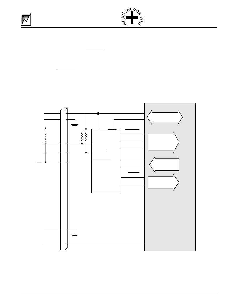
The board
’
s pins should now be mated with the backplane
connector which in turn will bring the host LI/I* and
RESET* signals to the S39421. These signals should be
tied to the device
’
s HST_PWR and HST_RST inputs
respectively. Whenever HST_PWR is low the outputs
controlling the backend power on sequencing will be
inhibited; it does not impact the reset outputs or reset
timer. When low, the HST_RST input will force the reset
outputs active; once it is released the reset timer will be
started and it will keep the reset outputs active for t
PURST
.
At the same time the signal pins are making contact, the
backend voltages are applied to the card (3.3V, 5V, +12V
and -12V on short pins), but, they are blocked by FETs
under the control of the S39421 (see figure 3 ). Depending
upon the state of the VSEL pin, the S39421 will monitor
either the bussed +5V only, the bussed +3.3V only or both
the bussed +5V and +3.3V. Once the S39421 has deter-
mined these supply voltages are at or above Vtrip, (and LI/
I* has released HST_PWR) it will release the VGATE
outputs and effectively turn them on at a rate equivalent
to 250V/second. At the same time it will force DRVREN
active thus providing power to the backend circuits.
FIGURE 25: GENERAL BLOCK DIAGRAM OF S39421 HOST BUS INTERFACE AND BACKEND SIGNAL INTERFACE
VGATE3
VGATE5
DRVREN
RESET
RESET
PND1
Gnd
Gnd
Vpc
Vpc
SGNL_VLD
HST_RST
HST_PWR
CARD3V
CARD5V
LI/O*
IL/I*
RESET*
Backend
Power Circuits
See Figure
Backend Voltage
to S39421
Monitor Circuits
Reset Control
of Backend
Circuits
Ejector Switch
Circuit
S39421
System
Vcc
VCC5
2024 ILL28.0
相關PDF資料 |
PDF描述 |
|---|---|
| S3954 | 76-element Si photodiode array High UV sensitivity photodiode array mounted in DIP |
| S3994-01 | Si PIN photodiode for optical power meters |
| S3AB | 3.0A SURFACE MOUNT GLASS PASSVATED RECTIFIER |
| S3MB | 3.0A FAST RECOVERY GLASS PASSIVATED RECTIFIER |
| S3KB | 3.0A FAST RECOVERY GLASS PASSIVATED RECTIFIER |
相關代理商/技術參數(shù) |
參數(shù)描述 |
|---|---|
| S394-90-108-00-760000 | 制造商:Mill-Max Mfg Corp 功能描述:Custom Socket |
| S3950G2NR | 制造商:TYAN 功能描述:1P/AMD,(2)LAN,PCI-X,(4)PCI,ATX - Trays |
| S3950G2NR RPL | 制造商:TYAN 功能描述:REPAIR/REPLACEMENT - Bulk |
| S3950G2NR-DF | 制造商:TYAN 功能描述:TYAN TOMCAT H1000S - Bulk |
| S3951BA | 制造商:Arcolectric 功能描述: |
發(fā)布緊急采購,3分鐘左右您將得到回復。