- 您現(xiàn)在的位置:買賣IC網(wǎng) > PDF目錄372108 > SA9025 (NXP SEMICONDUCTORS) 900 MHz transmit modulator and 2.2 GHz fractional-N synthesizer PDF資料下載
參數(shù)資料
| 型號: | SA9025 |
| 廠商: | NXP SEMICONDUCTORS |
| 元件分類: | 通信及網(wǎng)絡(luò) |
| 英文描述: | 900 MHz transmit modulator and 2.2 GHz fractional-N synthesizer |
| 中文描述: | SPECIALTY TELECOM CIRCUIT, PQFP48 |
| 封裝: | 7 X 7 X 1.40 MM, PLASTIC, LQFP-48 |
| 文件頁數(shù): | 21/23頁 |
| 文件大?。?/td> | 134K |
| 代理商: | SA9025 |

Philips Semiconductors
Objective specification
SA9025
900 MHz transmit modulator and 2.2 GHz
fractional–N synthesizer
1997 Aug 01
21
synthesizer. While in standby mode, the lock detect signal will be
forced to a valid lock state so that the lock detect signal will indicate
when the main and auxiliary phase detectors have achieved phase
lock.
Divide by M
The
÷
M is a 2-bit programmable divider which can be configured for
ney integer divide from 6 to 9. The divider is used to convert the
VCO output down to the reference frequency before feeding it into
the phase comparator.
VCO
This oscillator is used to generate the transmit IF frequency between
90MHz and 180MHz. The VCO tank is configured using a parallel
inductor tuning varactor diode. DC blocking capacitors are used to
isolate the varactor control voltage from the VCO tank DC bias
voltages.
SSB Up-converter and TX
IF
Buffer
The TX
IF
buffer provides isolation between the SSB Up-converter
and the VCO output. The Single Sideband Up-converter (SSB) is
an active Gilbert cell multiplier (matched pair), combined with two
quadrature phase shift networks and a low pass filter. The SSB
up-converter is used to reject the unwanted upper sideband that
would normally occur during the up-conversion process.
I/Q Modulator
The quadrature modulator is an active Gilbert cell multiplier
(matched pair) with cross coupled outputs. These outputs are then
provided to the variable gain amplifier. When the in-phase input I =
cos (
ω
t) and the quadrature-phase input Q = sin (
ω
t) (i.e., Q lags I
by 90
°
), the resulting output should be upper single sideband.
Variable Gain Amplifiers
The variable gain amplifiers are used to control the output level of
the device, with a power control range of 45.9dB. The output stages
are differential, matched from 200
to 50
.
Power Control
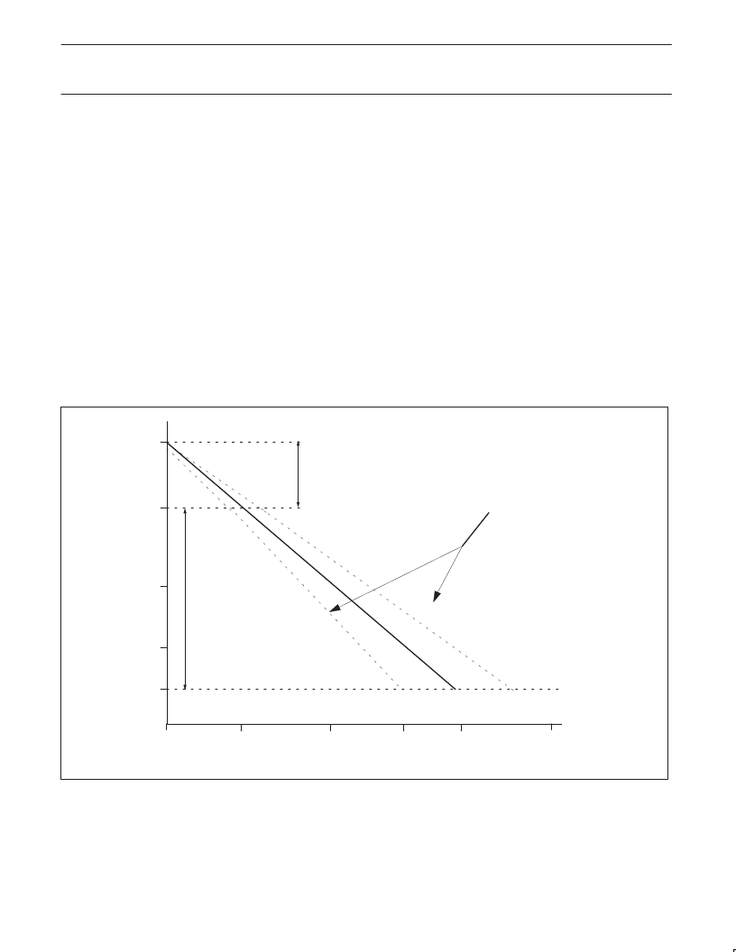
The power control range should be greater than or equal to 45.9dB,
having a monotonically decreasing slope, with 0dB = +11.5 dBm
nominal. Eight bits are available for power control programming.
The top 6 bits (PC7 to PC2) provide coarse attenuation with .6dB
step size accuracy. The bottom 2 bits provide fine attenuation with
.18 dB step size accuracy.
SR01453
MAXIMUM ACCUMULATED ERROR
(NOT TO SCALE)
TOP 12 dB FINE STEP ACURACY
BOTTOM 25 dB COARSE STEP AC-
CURACY
+11.5
–3
–15
–26
–28
0
12
24
38
45.9
VGA SETTING (dB)
P
Figure 11.
Power Control
Oscillator Buffers
There are three buffers for the reference signal, two of which are
used to provide external reference signals. The internal reference
signal is used for the main and auxiliary synthesizer reference. The
second buffer (MCLK) is used as a master clock for external digital
circuitry which is always on, while the third buffer (RCLK) is used as
a clock for external digital circuitry which is not used in sleep mode.
LO Buffers
The LO buffers are used to provide isolation for the VCO and
between the transmitter up-converter and channel synthesizer.
相關(guān)PDF資料 |
PDF描述 |
|---|---|
| SA910 | Variable gain RF predriver amplifier |
| SA9500 | Dual-band, CDMA/AMPS downconverter IC |
| SA9500DH | DD24661 |
| SA9502 | Dual-band, CDMA/AMPS downconverter IC |
| SA9502DH | Dual-band, CDMA/AMPS downconverter IC |
相關(guān)代理商/技術(shù)參數(shù) |
參數(shù)描述 |
|---|---|
| SA90A | 功能描述:TVS 二極管 - 瞬態(tài)電壓抑制器 SA90A Uni-Directional RoHS:否 制造商:Vishay Semiconductors 極性:Bidirectional 工作電壓: 擊穿電壓:58.9 V 鉗位電壓:77.4 V 峰值浪涌電流:38.8 A 系列: 封裝 / 箱體:DO-214AB 最小工作溫度:- 55 C 最大工作溫度:+ 150 C |
| SA90A _AY _10001 | 制造商:PanJit Touch Screens 功能描述: |
| SA90A/1 | 功能描述:TVS 二極管 - 瞬態(tài)電壓抑制器 500W 90V 5% Unidir RoHS:否 制造商:Vishay Semiconductors 極性:Bidirectional 工作電壓: 擊穿電壓:58.9 V 鉗位電壓:77.4 V 峰值浪涌電流:38.8 A 系列: 封裝 / 箱體:DO-214AB 最小工作溫度:- 55 C 最大工作溫度:+ 150 C |
| SA90A/4 | 功能描述:TVS 二極管 - 瞬態(tài)電壓抑制器 500W 90V 5% Unidir RoHS:否 制造商:Vishay Semiconductors 極性:Bidirectional 工作電壓: 擊穿電壓:58.9 V 鉗位電壓:77.4 V 峰值浪涌電流:38.8 A 系列: 封裝 / 箱體:DO-214AB 最小工作溫度:- 55 C 最大工作溫度:+ 150 C |
| SA90A/54 | 功能描述:TVS 二極管 - 瞬態(tài)電壓抑制器 500W 90V 5% Unidir RoHS:否 制造商:Vishay Semiconductors 極性:Bidirectional 工作電壓: 擊穿電壓:58.9 V 鉗位電壓:77.4 V 峰值浪涌電流:38.8 A 系列: 封裝 / 箱體:DO-214AB 最小工作溫度:- 55 C 最大工作溫度:+ 150 C |
發(fā)布緊急采購,3分鐘左右您將得到回復(fù)。