- 您現(xiàn)在的位置:買賣IC網(wǎng) > PDF目錄372108 > SAA2501H (NXP SEMICONDUCTORS) Digital Audio Broadcast DAB decoder PDF資料下載
參數(shù)資料
| 型號: | SAA2501H |
| 廠商: | NXP SEMICONDUCTORS |
| 元件分類: | 消費家電 |
| 英文描述: | Digital Audio Broadcast DAB decoder |
| 中文描述: | SPECIALTY CONSUMER CIRCUIT, PQFP44 |
| 封裝: | 10 X 10 MM, 1.75 MM HEIGHT, PLASTIC, SOT-307-2, QFP-44 |
| 文件頁數(shù): | 35/52頁 |
| 文件大小: | 206K |
| 代理商: | SAA2501H |
第1頁第2頁第3頁第4頁第5頁第6頁第7頁第8頁第9頁第10頁第11頁第12頁第13頁第14頁第15頁第16頁第17頁第18頁第19頁第20頁第21頁第22頁第23頁第24頁第25頁第26頁第27頁第28頁第29頁第30頁第31頁第32頁第33頁第34頁當(dāng)前第35頁第36頁第37頁第38頁第39頁第40頁第41頁第42頁第43頁第44頁第45頁第46頁第47頁第48頁第49頁第50頁第51頁第52頁

January 1995
35
Philips Semiconductors
Preliminary specification
Digital Audio Broadcast (DAB) decoder
SAA2501
8.1.1.2
Special function operational address
handbook, halfpage
0
1
2
3
4
5
6
7
L3CLK
L3DATA
MGB504
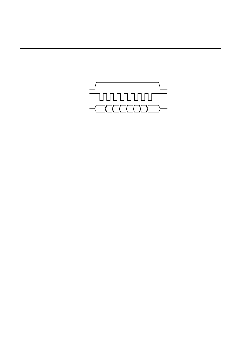
Fig.17 Data transfer mode.
Operational address 000000 (bit 2 to bit 7) is the special
function address, and is used for the L3 device reset, as
well as for the declaration and invalidation of the extended
addressing. Both will be explained in Sections 8.1.2 and
8.1.3.
8.1.1.3
Data mode
In the data mode (see Fig.17) the microcontroller sends or
receives information to or from the selected device. During
data transfer the L3MODE line is HIGH. The L3CLK line is
lowered 8 times during which the L3DATA line carries
8 bits. The information is presented LSB first and remains
stable during the LOW phase of the L3CLK signal.
The preferred basic data transfer unit is an 8 bit byte.
Some implementations that are modifications of earlier
circuits with 16 bit registers may use a basic unit of 16 bits,
transferred as 2 bytes, with the most significant byte
presented first. No other basic data transfer unit is allowed.
8.1.1.4
Halt mode
In between units the L3MODE line will be driven LOW by
the microcontroller to indicate the completion of a basic
unit transfer. This is called ‘halt mode’ (HM). During halt
mode the L3CLK line remains HIGH (to distinguish it from
an addressing mode). The halt mode allows an
implementation of an interface module without a bit
counter. However, an implementation using a bit counter
in the interface module may allow for the L3MODE line to
be kept HIGH in between units (not using the halt mode).
This implementation must also operate correctly if the halt
mode is used. The documentation of the device will have
to indicate clearly whether or not the ‘halt mode’ is
necessary for correct operation of the interface.
8.1.2
D
EVICE INTERFACE RESET
If the microcontroller sends an operational address
‘000000’ with DOM1 and DOM0 also equal to ‘0’ this
indicates that none of the L3 interface devices is allowed
to communicate with the microcontroller during the
following data mode. This enables a different application of
the L3CLK and L3DATA lines as the L3 devices will not
interfere with any communication on these lines as long as
L3MODE remains HIGH (e.g. the L3CLK and L3DATA
lines are normally connected to USART circuits in the
microcontrollers which allow for convenient
communication between microcontrollers).
Any addressing mode with a valid L3 operational address
will re-enable the communication with the corresponding
device.
Devices with a fixed operational address (‘Primary L3
devices’) will react with a device reset condition regardless
of the state of DOM1 and DOM0.
Devices with a programmable operational address
(‘Secondary L3 devices’) can only be put in the interface
reset condition if the DOM1 and DOM0 bits are ‘0’. Other
combinations of DOM1 and DOM0 initiate data transfers
for ‘extended addressing’.
8.1.3
E
XTENDED ADDRESSING
L3 Devices with a programmable address can be informed
of their operational address using a special data transfer.
相關(guān)PDF資料 |
PDF描述 |
|---|---|
| SAA2502 | ISO/MPEG Audio Source Decoder |
| SAA2502H | ISO/MPEG Audio Source Decoder |
| SAA2503 | MPEG2 audio decoder(MPEG2 音頻譯碼器) |
| SAA2503HT | MPEG2 audio decoder |
| SAA2505H-M1 | Digital multi-channel audio IC DUET |
相關(guān)代理商/技術(shù)參數(shù) |
參數(shù)描述 |
|---|---|
| SAA2501HB-S | 制造商:未知廠家 制造商全稱:未知廠家 功能描述:Digital Audio Decoder & Support |
| SAA2502 | 制造商:PHILIPS 制造商全稱:NXP Semiconductors 功能描述:ISO/MPEG Audio Source Decoder |
| SAA2502H | 制造商:PHILIPS 制造商全稱:NXP Semiconductors 功能描述:ISO/MPEG Audio Source Decoder |
| SAA2503 | 制造商:PHILIPS 制造商全稱:NXP Semiconductors 功能描述:MPEG2 audio decoder |
| SAA2503HT | 制造商:PHILIPS 制造商全稱:NXP Semiconductors 功能描述:MPEG2 audio decoder |
發(fā)布緊急采購,3分鐘左右您將得到回復(fù)。