- 您現(xiàn)在的位置:買賣IC網(wǎng) > PDF目錄373435 > SN74ABT8374 (Texas Instruments, Inc.) Scan Test Devices With Octal D-Type Edge-Triggered Flip-Flops(掃描測試裝置(帶八D邊沿觸發(fā)器)) PDF資料下載
參數(shù)資料
| 型號: | SN74ABT8374 |
| 廠商: | Texas Instruments, Inc. |
| 英文描述: | Scan Test Devices With Octal D-Type Edge-Triggered Flip-Flops(掃描測試裝置(帶八D邊沿觸發(fā)器)) |
| 中文描述: | 掃描測試設(shè)備與八路D型邊沿觸發(fā)正反器(掃描測試裝置(帶八?邊沿觸發(fā)器)) |
| 文件頁數(shù): | 13/19頁 |
| 文件大小: | 391K |
| 代理商: | SN74ABT8374 |
SN54ABT8374, SN74ABT8374
SCAN TEST DEVICES WITH
OCTAL D-TYPE EDGE-TRIGGERED FLIP-FLOPS
SCBS486 – JULY 1994
3–13
POST OFFICE BOX 655303
DALLAS, TEXAS 75265
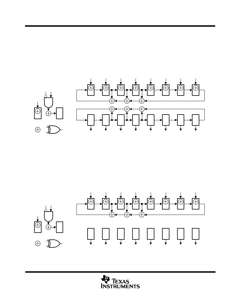
simultaneous PSA and PRPG (PSA/PRPG)
Data appearing at the device input pins is compressed into an 8-bit parallel signature in the shift-register
elements of the input BSCs on each rising edge of TCK. This data is then updated in the shadow latches of the
input BSCs and applied to the inputs of the normal on-chip logic. At the same time, an 8-bit pseudo-random
pattern is generated in the shift-register elements of the output BSCs on each rising edge of TCK, updated in
the shadow latches, and applied to the device output pins on each falling edge of TCK. Figure 7 illustrates the
8-bit linear-feedback shift-register algorithms through which the signature and patterns are generated. An initial
seed value should be scanned into the BSR before performing this operation. A seed value of all zeroes does
not produce additional patterns.
=
=
M
8D
8Q
7D
6D
5D
4D
3D
2D
1D
7Q
6Q
5Q
4Q
3Q
2Q
1Q
Figure 6. 8-Bit PSA/PRPG Configuration
simultaneous PSA and binary count up (PSA/COUNT)
Data appearing at the device input pins is compressed into an 8-bit parallel signature in the shift-register
elements of the input BSCs on each rising edge of TCK. This data is then updated in the shadow latches of the
input BSCs and applied to the inputs of the normal on-chip logic. At the same time, an 8-bit binary count-up
pattern is generated in the shift-register elements of the output BSCs on each rising edge of TCK updated in
the shadow latches, and applied to the device output pins on each falling edge of TCK. Figure 8 illustrates the
8-bit linear-feedback shift-register algorithm through which the signature is generated. An initial seed value
should be scanned into the BSR before performing this operation.
=
=
M
8D
8Q
7D
6D
5D
4D
3D
2D
1D
7Q
6Q
5Q
4Q
3Q
2Q
1Q
MSB
LSB
Figure 7. 8-Bit PSA/COUNT Configuration
P
相關(guān)PDF資料 |
PDF描述 |
|---|---|
| SN54ABT845 | Octal Bus Interface D-Type Latches With 3-State Outputs(八總線接口D鎖存器(三態(tài)輸出)) |
| SN74ABT845 | Octal Bus Interface D-Type Latches With 3-State Outputs(八總線接口D觸發(fā)器(三態(tài)輸出)) |
| SN54ABT8543FK | SCAN TEST DEVICES WITH OCTAL REGISTERED BUS TRANSCEIVERS |
| SN54ABT8543JT | SCAN TEST DEVICES WITH OCTAL REGISTERED BUS TRANSCEIVERS |
| SN54ABT854 | 8-Bit To 9-Bit Parity Bus Transceivers(8-9奇偶總線收發(fā)器) |
相關(guān)代理商/技術(shù)參數(shù) |
參數(shù)描述 |
|---|---|
| SN74ABT841ADBR | 功能描述:閉鎖 10bit Bus D RoHS:否 制造商:Micrel 電路數(shù)量:1 邏輯類型:CMOS 邏輯系列:TTL 極性:Non-Inverting 輸出線路數(shù)量:9 高電平輸出電流: 低電平輸出電流: 傳播延遲時(shí)間: 電源電壓-最大:12 V 電源電壓-最小:5 V 最大工作溫度:+ 85 C 最小工作溫度:- 40 C 封裝 / 箱體:SOIC-16 封裝:Reel |
| SN74ABT841ADBRE4 | 功能描述:閉鎖 10bit Bus D RoHS:否 制造商:Micrel 電路數(shù)量:1 邏輯類型:CMOS 邏輯系列:TTL 極性:Non-Inverting 輸出線路數(shù)量:9 高電平輸出電流: 低電平輸出電流: 傳播延遲時(shí)間: 電源電壓-最大:12 V 電源電壓-最小:5 V 最大工作溫度:+ 85 C 最小工作溫度:- 40 C 封裝 / 箱體:SOIC-16 封裝:Reel |
| SN74ABT841ADBRG4 | 功能描述:閉鎖 10B Bus-Interface D-Type RoHS:否 制造商:Micrel 電路數(shù)量:1 邏輯類型:CMOS 邏輯系列:TTL 極性:Non-Inverting 輸出線路數(shù)量:9 高電平輸出電流: 低電平輸出電流: 傳播延遲時(shí)間: 電源電壓-最大:12 V 電源電壓-最小:5 V 最大工作溫度:+ 85 C 最小工作溫度:- 40 C 封裝 / 箱體:SOIC-16 封裝:Reel |
| SN74ABT841ADW | 功能描述:閉鎖 10bit Bus D RoHS:否 制造商:Micrel 電路數(shù)量:1 邏輯類型:CMOS 邏輯系列:TTL 極性:Non-Inverting 輸出線路數(shù)量:9 高電平輸出電流: 低電平輸出電流: 傳播延遲時(shí)間: 電源電壓-最大:12 V 電源電壓-最小:5 V 最大工作溫度:+ 85 C 最小工作溫度:- 40 C 封裝 / 箱體:SOIC-16 封裝:Reel |
| SN74ABT841ADWG4 | 功能描述:閉鎖 10B Bus-Interface D-Type RoHS:否 制造商:Micrel 電路數(shù)量:1 邏輯類型:CMOS 邏輯系列:TTL 極性:Non-Inverting 輸出線路數(shù)量:9 高電平輸出電流: 低電平輸出電流: 傳播延遲時(shí)間: 電源電壓-最大:12 V 電源電壓-最小:5 V 最大工作溫度:+ 85 C 最小工作溫度:- 40 C 封裝 / 箱體:SOIC-16 封裝:Reel |
發(fā)布緊急采購,3分鐘左右您將得到回復(fù)。