- 您現(xiàn)在的位置:買賣IC網(wǎng) > PDF目錄378747 > UPD75336GK (NEC Corp.) 4-BIT SINGLE-CHIP MICROCOMPUTER PDF資料下載
參數(shù)資料
| 型號: | UPD75336GK |
| 廠商: | NEC Corp. |
| 英文描述: | 4-BIT SINGLE-CHIP MICROCOMPUTER |
| 中文描述: | 4位單片機 |
| 文件頁數(shù): | 47/68頁 |
| 文件大小: | 532K |
| 代理商: | UPD75336GK |
第1頁第2頁第3頁第4頁第5頁第6頁第7頁第8頁第9頁第10頁第11頁第12頁第13頁第14頁第15頁第16頁第17頁第18頁第19頁第20頁第21頁第22頁第23頁第24頁第25頁第26頁第27頁第28頁第29頁第30頁第31頁第32頁第33頁第34頁第35頁第36頁第37頁第38頁第39頁第40頁第41頁第42頁第43頁第44頁第45頁第46頁當前第47頁第48頁第49頁第50頁第51頁第52頁第53頁第54頁第55頁第56頁第57頁第58頁第59頁第60頁第61頁第62頁第63頁第64頁第65頁第66頁第67頁第68頁
47
μ
PD75336
MAIN SYSTEM CLOCK OSCILLATOR CHARACTERISTICS (Ta = –40 to +85
°
C, V
DD
= 2.7 to 6.0 V)
RECOMMENDED
CIRCUIT
TEST
RESONATOR
PARAMETER
MIN.
TYP.
MAX.
UNIT
CONDITIONS
Oscillator
frequency (f
x
)
*1
After V
DD
reaches the
MIN. value of
the oscillation
voltage
range
Oscillation
stabilization time
*2
Oscillator
frequency (f
x
)
*1
V
DD
= 4.5
to 6.0 V
Oscillation
stabilization time
*2
30
ms
X1 input
frequency (f
x
)
*1
X1 input
high-/low-level
width (t
XH
, t
XL
)
100
500
ns
4
ms
1.0
5.0
*3
MHz
1.0
4.19
5.0
*3
MHz
1.0
5.0
*3
MHz
10
ms
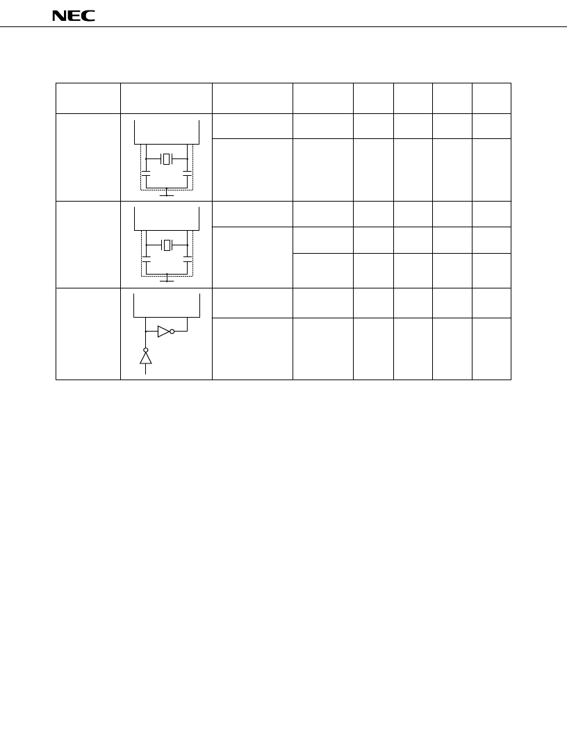
Ceramic
resonator
Crystal
resonator
External
clock
X1
X2
C2
C1
V
DD
X1
X2
C2
C1
V
DD
X1
X2
μ
PD74HCU04
*
1.
The oscillator frequency and X1 input frequency indicate only the oscillator characteristics. For the instruction
execution time refer to the AC CHARACTERISTICS.
2.
The oscillation stabilization time is necessary for oscillation to stabilize after V
DD
reaches the MIN. value of
the oscillation voltage range or releasing the STOP mode.
3.
When the oscillator frequency is “4.19 MHz < f
X
≤
5.0 MHz” PCC = 0011 should for the instruction execution
time. If PCC = 0011 is selection, 1 machine cycle is less than 0.95
μ
s with the result that the specified MIN.
value, 0.95
μ
s cannot be observed.
Note
When using the main system clock oscillator or the subsystem clock oscillator, wiring in the area enclosed
with the dotted line should be carried out as follows to avoid an adverse effect from wiring capacitance.
Wiring should be as short as possible.
Wiring should not cross other signal lines or not be placed close to a varying high current.
The potential of the oscillator capacitor ground should always be the same as V
SS
. Do not ground wiring
to a ground pattern in which a high current flows.
Do not fetch a signal from the oscillator.
The subsystem clock oscillator is a circuit with a low amplification level, more prone to misoperation due
to noise than the main system clock. Therefore, when using the subsystem clock, special care is required
in wiring methods.
#
相關(guān)PDF資料 |
PDF描述 |
|---|---|
| UPD75336 | 4-BIT SINGLE-CHIP MICROCOMPUTER |
| UPD754244 | 4-BIT SINGLE-CHIP MICROCONTROLLERS |
| UPD754244GS | 4-BIT SINGLE-CHIP MICROCONTROLLERS |
| UPD75512 | 4-BIT SINGLE-CHIP MICROCOMPUTER |
| UPD75512A | 4-BIT SINGLE-CHIP MICROCOMPUTER |
相關(guān)代理商/技術(shù)參數(shù) |
參數(shù)描述 |
|---|---|
| UPD7554AG-597-E2 | 制造商:Renesas Electronics Corporation 功能描述: |
| UPD7554AG-597-E2-A | 制造商:Renesas Electronics Corporation 功能描述: |
| UPD7554AG-603-E2 | 制造商:Renesas Electronics Corporation 功能描述: |
| UPD7554AG-603-E2-A | 制造商:Renesas Electronics Corporation 功能描述: |
| UPD7554AG-611-E2 | 制造商:Renesas Electronics Corporation 功能描述: |
發(fā)布緊急采購,3分鐘左右您將得到回復(fù)。