- 您現(xiàn)在的位置:買賣IC網(wǎng) > PDF目錄378747 > UPD75517GF (NEC Corp.) 4 BIT SINGLE-CHIP MICROCOMPUTER PDF資料下載
參數(shù)資料
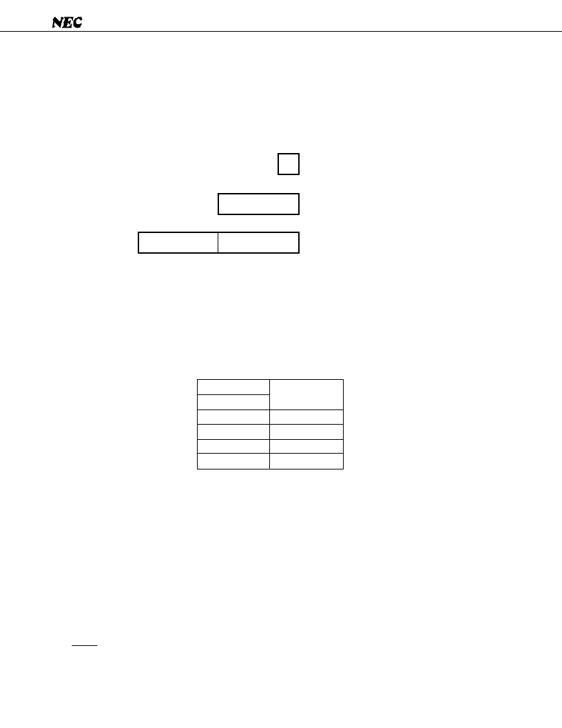
| 型號(hào): | UPD75517GF |
| 廠商: | NEC Corp. |
| 英文描述: | 4 BIT SINGLE-CHIP MICROCOMPUTER |
| 中文描述: | 4位單片機(jī) |
| 文件頁(yè)數(shù): | 32/180頁(yè) |
| 文件大?。?/td> | 1596K |
| 代理商: | UPD75517GF |
第1頁(yè)第2頁(yè)第3頁(yè)第4頁(yè)第5頁(yè)第6頁(yè)第7頁(yè)第8頁(yè)第9頁(yè)第10頁(yè)第11頁(yè)第12頁(yè)第13頁(yè)第14頁(yè)第15頁(yè)第16頁(yè)第17頁(yè)第18頁(yè)第19頁(yè)第20頁(yè)第21頁(yè)第22頁(yè)第23頁(yè)第24頁(yè)第25頁(yè)第26頁(yè)第27頁(yè)第28頁(yè)第29頁(yè)第30頁(yè)第31頁(yè)當(dāng)前第32頁(yè)第33頁(yè)第34頁(yè)第35頁(yè)第36頁(yè)第37頁(yè)第38頁(yè)第39頁(yè)第40頁(yè)第41頁(yè)第42頁(yè)第43頁(yè)第44頁(yè)第45頁(yè)第46頁(yè)第47頁(yè)第48頁(yè)第49頁(yè)第50頁(yè)第51頁(yè)第52頁(yè)第53頁(yè)第54頁(yè)第55頁(yè)第56頁(yè)第57頁(yè)第58頁(yè)第59頁(yè)第60頁(yè)第61頁(yè)第62頁(yè)第63頁(yè)第64頁(yè)第65頁(yè)第66頁(yè)第67頁(yè)第68頁(yè)第69頁(yè)第70頁(yè)第71頁(yè)第72頁(yè)第73頁(yè)第74頁(yè)第75頁(yè)第76頁(yè)第77頁(yè)第78頁(yè)第79頁(yè)第80頁(yè)第81頁(yè)第82頁(yè)第83頁(yè)第84頁(yè)第85頁(yè)第86頁(yè)第87頁(yè)第88頁(yè)第89頁(yè)第90頁(yè)第91頁(yè)第92頁(yè)第93頁(yè)第94頁(yè)第95頁(yè)第96頁(yè)第97頁(yè)第98頁(yè)第99頁(yè)第100頁(yè)第101頁(yè)第102頁(yè)第103頁(yè)第104頁(yè)第105頁(yè)第106頁(yè)第107頁(yè)第108頁(yè)第109頁(yè)第110頁(yè)第111頁(yè)第112頁(yè)第113頁(yè)第114頁(yè)第115頁(yè)第116頁(yè)第117頁(yè)第118頁(yè)第119頁(yè)第120頁(yè)第121頁(yè)第122頁(yè)第123頁(yè)第124頁(yè)第125頁(yè)第126頁(yè)第127頁(yè)第128頁(yè)第129頁(yè)第130頁(yè)第131頁(yè)第132頁(yè)第133頁(yè)第134頁(yè)第135頁(yè)第136頁(yè)第137頁(yè)第138頁(yè)第139頁(yè)第140頁(yè)第141頁(yè)第142頁(yè)第143頁(yè)第144頁(yè)第145頁(yè)第146頁(yè)第147頁(yè)第148頁(yè)第149頁(yè)第150頁(yè)第151頁(yè)第152頁(yè)第153頁(yè)第154頁(yè)第155頁(yè)第156頁(yè)第157頁(yè)第158頁(yè)第159頁(yè)第160頁(yè)第161頁(yè)第162頁(yè)第163頁(yè)第164頁(yè)第165頁(yè)第166頁(yè)第167頁(yè)第168頁(yè)第169頁(yè)第170頁(yè)第171頁(yè)第172頁(yè)第173頁(yè)第174頁(yè)第175頁(yè)第176頁(yè)第177頁(yè)第178頁(yè)第179頁(yè)第180頁(yè)
32
μ
PD75517(A)
3.5 ACCUMULATORS
In the
μ
PD75517(A), the A register and the XA register pair function as accumulators. The A register is mainly
used for 4-bit data processing instructions, and the XA register pair is mainly used for 8-bit data processing
instructions.
For a bit manipulation instruction, the carry flag (CY) functions as a bit accumulator.
Fig. 3-6 Accumulators
3.6 STACK POINTER (SP) AND STACK BANK SELECT REGISTER (SBS)
The
μ
PD75517(A) uses static RAM as stack memory (LIFO scheme), and the 8-bit register holding the start
address of the stack area is the stack pointer (SP).
The stack area is located at addresses 000H to 3FFH in memory banks 0, 1, 2, and 3. Either of the memory
banks is selected according to the value of the 2-bit SBS. (See
Table 3-1
.)
Table 3-1 Stack Area to Be Selected by the SBS
The SP is decremented before a write (save) operation to stack memory, and is incremented after a read
(restoration) operation from stack memory. The SBS is set with a 4-bit memory manipulation instruction. Note
that the high-order two bits are always set to 00.
Fig. 3-8 and 3-9 show data saved to and restored from stack memory in these stack operations.
To place the stack area at a given location, the SP can be initialized with an 8-bit memory manipulation
instruction, and the SBS can be initialized with a 4-bit memory manipulation instruction. Both can be read
from as well.
When the SP is initialized to 00H, a stack operation starts at the high-order address (nFFH) of memory bank
(n) specified with the SBS.
A stack area must be within the memory bank specified with the SBS. If a stack operation exceeds address
n00H, the operation returns to address nFFH of the same bank. Stacking beyond memory bank boundaries
is enabled only by resetting the SBS.
A RESET signal occurrence causes the contents of the SP and the SBS to be undefined, so that the SP must
always be initialized to a desired value at the start of the program.
Bit accumulator
4-bit accumulator
8-bit accumulator
CY
A
A
X
SBS2
0
1
0
1
SBS
Memory bank 0
Memory bank 1
Memory bank 2
Memory bank 3
Stack area
-
SBS1
0
0
1
1
相關(guān)PDF資料 |
PDF描述 |
|---|---|
| UPD75517GFA | 4 BIT SINGLE-CHIP MICROCOMPUTER |
| UPD75518 | 4 BIT SINGLE-CHIP MICROCOMPUTER |
| UPD75518GF | CAT5E PATCH CABLES SNAGLESS, RED 3 FT |
| UPD75518GFA | 4 BIT SINGLE-CHIP MICROCOMPUTER |
| UPD75518A | 4 BIT SINGLE-CHIP MICROCOMPUTER |
相關(guān)代理商/技術(shù)參數(shù) |
參數(shù)描述 |
|---|---|
| UPD7554AG-597-E2 | 制造商:Renesas Electronics Corporation 功能描述: |
| UPD7554AG-597-E2-A | 制造商:Renesas Electronics Corporation 功能描述: |
| UPD7554AG-603-E2 | 制造商:Renesas Electronics Corporation 功能描述: |
| UPD7554AG-603-E2-A | 制造商:Renesas Electronics Corporation 功能描述: |
| UPD7554AG-611-E2 | 制造商:Renesas Electronics Corporation 功能描述: |
發(fā)布緊急采購(gòu),3分鐘左右您將得到回復(fù)。