- 您現(xiàn)在的位置:買賣IC網(wǎng) > PDF目錄379508 > UPD98404GJ-KEU (NEC Corp.) E Core PDF資料下載
參數(shù)資料
| 型號: | UPD98404GJ-KEU |
| 廠商: | NEC Corp. |
| 英文描述: | E Core |
| 中文描述: | 高級自動柜員機的SONET成幀器 |
| 文件頁數(shù): | 11/36頁 |
| 文件大小: | 201K |
| 代理商: | UPD98404GJ-KEU |
第1頁第2頁第3頁第4頁第5頁第6頁第7頁第8頁第9頁第10頁當(dāng)前第11頁第12頁第13頁第14頁第15頁第16頁第17頁第18頁第19頁第20頁第21頁第22頁第23頁第24頁第25頁第26頁第27頁第28頁第29頁第30頁第31頁第32頁第33頁第34頁第35頁第36頁
Data Sheet S11822EJ4V0DS00
11
μ
PD98404
(3/3)
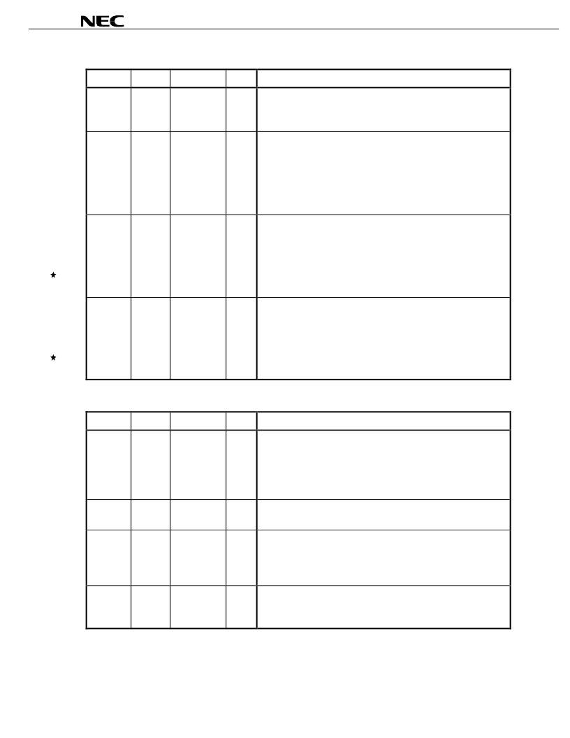
Pin name
Pin No.
I/O level
I/O
Function
TxFP
14
TTL*
O
Frame pulse signal output for the transmit side (8 kHz). This pin
outputs a pulse signal at one-clock intervals in sync with the TCL
clock.
TFSS
13
TTL*
I
Transmit frame output disable signal input. When the signal is high,
the transmit frame output stops. When the signal is low, transmission
starts from the beginning of a frame. The
μ
PD98404 samples this
signal at the rising edge of the TCL clock. The transmit frame output
is resumed at the ninth rising edge of the TCL clock after the rising
edge at which the high level of this signal was last detected.
RCL
75
TTL*
O
Internal system clock output for the receive side (19.44 MHz). This
pin outputs the receive clock divided by 8. The source receive clock
depends on the selected mode, which is either the clock generated by
the internal clock recovery PLL or the clock supplied from the
RCIT/RCIC and RFC pins. Clock output from this pin is stopped while
the device is being reset.
TCL
15
TTL*
O
Internal system clock output of the transmit side (19.44 MHz).
This pin outputs the transmit clock divided by 8. The source transmit
clock depends on the selected mode, which is either the clock
generated by the internal synthesizer or the clock supplied from the
TCIT/TCIC and TFC pins. Clock output from this pin is stopped while
the device is being reset.
1.2
ATM layer interface
(1/2)
Pin name
Pin No.
I/O level
I/O
Function
RDO0-
RDO7
130-137
TTL*
O
(2 or 3-
state)
Receive data output.
These pins form an 8-bit data bus that outputs receive data to an ATM
layer device. The data is output in sync with the rising edge of the
RCLK clock. These pins operate in two or three states, depending on
the UTOPIA interface mode.
RCLK
128
TTL*
I
Receive clock input. This pin supplies a clock of up to 40 MHz for
receive data transfer.
RSOC
126
TTL*
O
(2 or 3-
state)
Receive cell start position signal output.
This pin outputs a signal indicating the position of the first byte of a
receive cell. This pin operates in two or three states, depending on
the UTOPIA interface mode.
RENBL_B
127
TTL*
I
Receive enable signal input.
This pin inputs a signal indicating that the ATM layer is ready to
receive data.
相關(guān)PDF資料 |
PDF描述 |
|---|---|
| UPD98404 | Ultraframer DS3/E3/DS2/E2/DS1/E1/DS0 |
| UPF01002 | Ultraframer DS3/E3/DS2/E2/DS1/E1/DS0 |
| UPG137GV-E1 | CRYSTAL 20.0 MHZ 20PF SMD |
| UPG137GV | L-BAND SPDT SWITCH |
| UPG138GV-E1 | CRYSTAL 24.0 MHZ 20PF SMD |
相關(guān)代理商/技術(shù)參數(shù) |
參數(shù)描述 |
|---|---|
| UPD98405 | 制造商:NEC 制造商全稱:NEC 功能描述:155M ATM INTEGRATED SAR CONTROLLER |
| UPD98405GL-PMU | 制造商:NEC 制造商全稱:NEC 功能描述:155M ATM INTEGRATED SAR CONTROLLER |
| UPD98408 | 制造商:未知廠家 制造商全稱:未知廠家 功能描述:Peripheral Miscellaneous |
| UPD98408GD-LML | 制造商:未知廠家 制造商全稱:未知廠家 功能描述:ATM DATA-LINK SWITCHING/ROUTING|CMOS|QFP|208PIN|PLASTIC |
| UPD98409 | 制造商:NEC 制造商全稱:NEC 功能描述:ATM LIGHT SAR CONTROLLER |
發(fā)布緊急采購,3分鐘左右您將得到回復(fù)。