- 您現(xiàn)在的位置:買賣IC網(wǎng) > PDF目錄359354 > VDP3104B (MICRONAS SEMICONDUCTOR HOLDING AG) Video Processor Family PDF資料下載
參數(shù)資料
| 型號: | VDP3104B |
| 廠商: | MICRONAS SEMICONDUCTOR HOLDING AG |
| 元件分類: | 消費(fèi)家電 |
| 英文描述: | Video Processor Family |
| 中文描述: | SPECIALTY CONSUMER CIRCUIT, PDIP64 |
| 封裝: | SHRINK, PLASTIC, DIP-64 |
| 文件頁數(shù): | 35/72頁 |
| 文件大小: | 603K |
| 代理商: | VDP3104B |
第1頁第2頁第3頁第4頁第5頁第6頁第7頁第8頁第9頁第10頁第11頁第12頁第13頁第14頁第15頁第16頁第17頁第18頁第19頁第20頁第21頁第22頁第23頁第24頁第25頁第26頁第27頁第28頁第29頁第30頁第31頁第32頁第33頁第34頁當(dāng)前第35頁第36頁第37頁第38頁第39頁第40頁第41頁第42頁第43頁第44頁第45頁第46頁第47頁第48頁第49頁第50頁第51頁第52頁第53頁第54頁第55頁第56頁第57頁第58頁第59頁第60頁第61頁第62頁第63頁第64頁第65頁第66頁第67頁第68頁第69頁第70頁第71頁第72頁
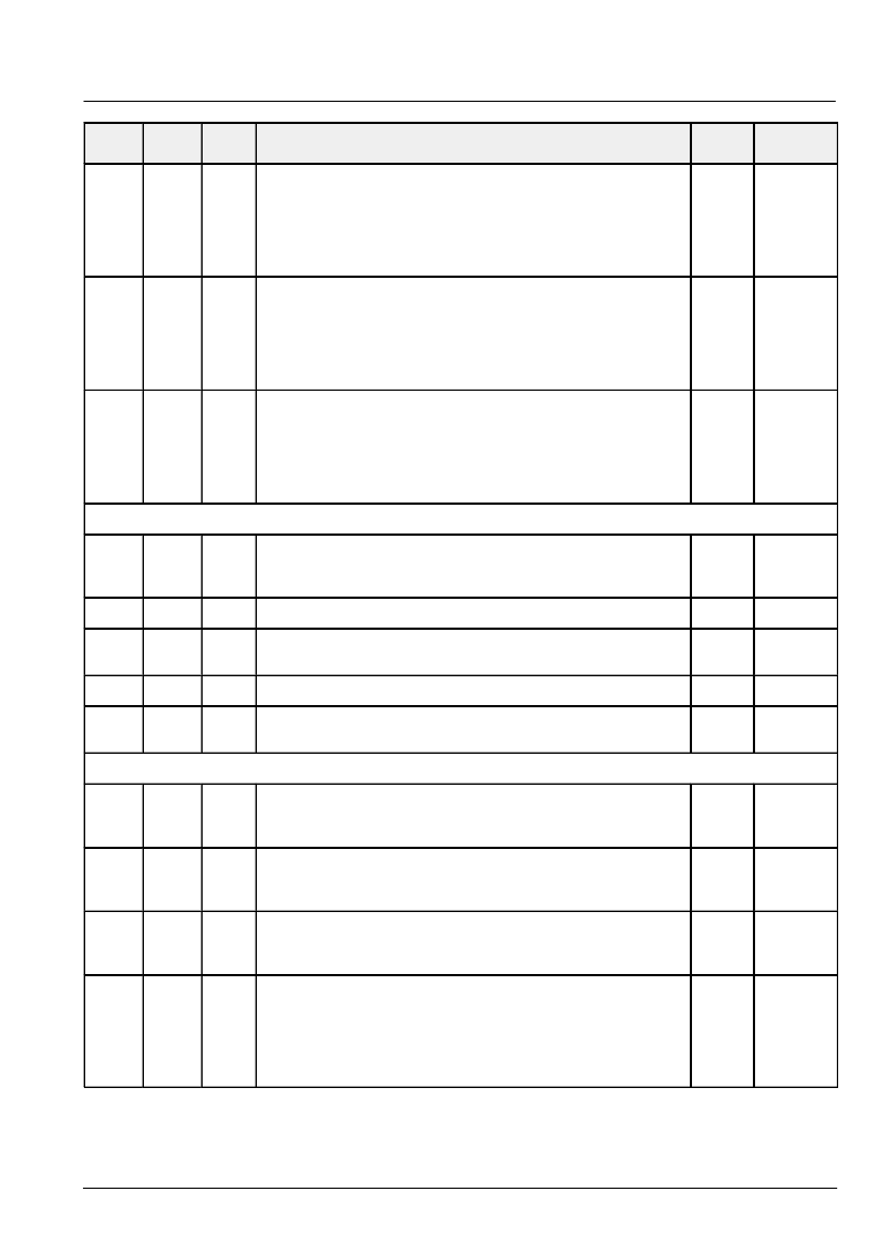
VDP 31xxB
PRELIMINARY DATA SHEET
35
Micronas
Name
Default
Function
Mode
Number
of bits
I
2
C sub
address
h
’
4c
9
w v
digital OSD insertion contrast for R (amplitude range: 0 to 255)
bit [3:0]
0..13
R amplitude = CLUTn
·
(DRCT + 4)
14,15
invalid
picture frame insertion contrast for R (ampl. range: 0 to 255)
bit [7:4]
0..13
R amplitude = PFCR
·
(PFRCT + 4)
14,15
invalid
8
8
DRCT
PFRCT
h
’
48
9
w v
digital OSD insertion contrast for G (amplitude range: 0 to 255)
bit [3:0]
0..13
G amplitude = CLUTn
·
(DGCT + 4)
14,15
invalid
picture frame insertion contrast for G (ampl. range: 0 to 255)
bit [7:4]
0..13
G amplitude = PFCG
·
(PFGCT + 4)
14,15
invalid
8
8
DGCT
PFGCT
h
’
44
9
w v
digital OSD insertion contrast for B (amplitude range: 0 to 255)
bit [3:0]
0..13
B amplitude = CLUTn
·
(DBCT + 4)
14,15
invalid
picture frame insertion contrast for B (ampl. range: 0 to 255)
bit [7:4]
0..13
B amplitude = PFCB
·
(PFBCT + 4)
14,15
invalid
8
8
DBCT
PFBCT
PICTURE FRAME GENERATOR
h
’
4F
9
w v
bit [8:0] horizontal picture frame begin
code 0 = picture frame generator horizontally disabled
code 1FF = full frame
0
PFGHB
h
’
53
9
w v
bit [8:0] horizontal picture frame end
0
PFGHE
h
’
63
9
w v
bit [8:0] vertical picture frame begin
code 0 = picture frame generator vertically disabled
270
PFGVB
h
’
6f
9
w v
bit [8:0] vertical picture frame end
56
PFGVE
enable and priority
–
see under
‘
PRIORITY BUS
’
picture frame color
–
see under
‘
COLOR LOOK-UP TABLE
’
SCAN VELOCITY MODULATION
h
’
62
9
w v
video mode coefficients
bit [5:0]
gain1
bit [8:6]
differentiator delay 1 (0= filter off, 1...6= delay)
60
4
SVG1
SVD1
h
’
5e
9
w v
text mode coefficients
bit [5:0]
bit [8:6]
gain 2
differentiator delay 2 (0= filter off, 1...6= delay)
60
4
SVG2
SVD2
h
’
5a
9
w v
limiter
bit [6:0]
bit [8:5]
limit value
not used, set to
”
0
”
100
0
SVLIM
h
’
56
9
w v
delay and coring
bit [3:0]
adjustable delay, in 1/2 display clock steps,
(value 5 : delay of SVMOUT is the same as for
RGBOUT
coring value
not used, set to
”
0
”
bit [7:4]
bit [8]
7
0
SVDEL
SVCOR
相關(guān)PDF資料 |
PDF描述 |
|---|---|
| VDP3108 | Single-Chip Video Processor |
| VDP3130Y | Video Processor Family |
| VDP31XXB | Video Processor Family |
| VDP3108PR | Consumer IC |
| VDSGLD_38.88 | TRANS PREBIASED PNP 200MW SOT23 |
相關(guān)代理商/技術(shù)參數(shù) |
參數(shù)描述 |
|---|---|
| VDP3108 | 制造商:MICRONAS 制造商全稱:MICRONAS 功能描述:Single-Chip Video Processor |
| VDP3108B | 制造商:MICRONAS 制造商全稱:MICRONAS 功能描述:Video Processor Family |
| VDP3108PR | 制造商:未知廠家 制造商全稱:未知廠家 功能描述:Consumer IC |
| VDP3112B | 制造商:MICRONAS 制造商全稱:MICRONAS 功能描述:Video Processor Family |
| VDP3116B | 制造商:MICRONAS 制造商全稱:MICRONAS 功能描述:Video Processor Family |
發(fā)布緊急采購,3分鐘左右您將得到回復(fù)。