- 您現(xiàn)在的位置:買賣IC網(wǎng) > PDF目錄203626 > W3E16M64S-250BC (MICROSEMI CORP-PMG MICROELECTRONICS) 16M X 64 DDR DRAM, 0.8 ns, PBGA219 PDF資料下載
參數(shù)資料
| 型號(hào): | W3E16M64S-250BC |
| 廠商: | MICROSEMI CORP-PMG MICROELECTRONICS |
| 元件分類: | DRAM |
| 英文描述: | 16M X 64 DDR DRAM, 0.8 ns, PBGA219 |
| 封裝: | 21 X 25 MM, PLASTIC, BGA-219 |
| 文件頁數(shù): | 13/16頁 |
| 文件大小: | 406K |
| 代理商: | W3E16M64S-250BC |
6
White Electronic Designs Corporation (602) 437-1520 www.whiteedc.com
White Electronic Designs
W3E16M64S-XBX
January 2008
Rev. 5
EXTENDED MODE REGISTER
The extended mode register controls functions beyond
those controlled by the mode register; these additional
functions are DLL enable/disable, output drive strength,
and QFC#. These functions are controlled via the bits
shown in Figure 5. The extended mode register is
programmed via the LOAD MODE REGISTER command
to the mode register (with BA0 = 1 and BA1 = 0) and
will retain the stored information until it is programmed
again or the device loses power. The enabling of the DLL
should always be followed by a LOAD MODE REGISTER
command to the mode register (BA0/BA1 both LOW) to
reset the DLL.
The extended mode register must be loaded when all
banks are idle and no bursts are in progress, and the
controller must wait the specied time before initiating
any subsequent operation. Violating either of these
requirements could result in unspecied operation.
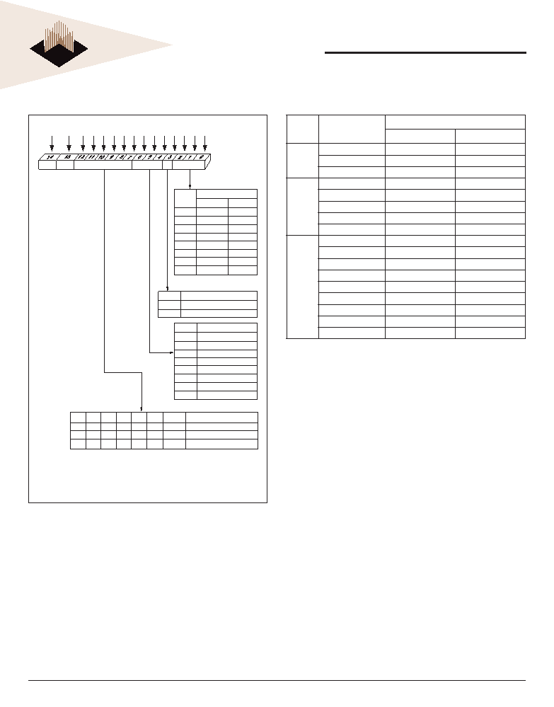
TABLE 1 – BURST DEFINITION
FIGURE 3 – MODE REGISTER DEFINITION
M3 = 0
2
4
8
Reserved
M3 = 1
2
4
8
Reserved
Operating Mode
Normal Operation
Normal Operation/Reset DLL
All other states reserved
00
Valid
0
1
Burst Type
Sequential
Interleaved
CAS Latency
Reserved
2
Reserved
2.5
Reserved
Burst Length
M0
0
1
0
1
0
1
0
1
Burst Length
CAS Latency
BT
A9
A7
A6
A5
A4
A3
A8
A2
A1
A0
Mode Register (Mx)
Address Bus
M1
0
1
0
1
M2
0
1
M3
M4
0
1
0
1
0
1
0
1
M5
0
1
0
1
M6
0
1
M6-M0
M8
M7
Operating Mode
A10
A11
* M14 and M13
(BA0 and BA1 must be
"0, 0" to select
the base mode register
(vs. the extended
mode register).
0*
BA0
BA1
Reserved
M9
M10
M11
0
10
0
--
-
A12
M12
0
-
Burst
Length
Starting Column
Address
Order of Accesses Within a Burst
Type = Sequential
Type = Interleaved
2
A0
0
0-1
1
1-0
4
A1
A0
0
0-1-2-3
0
1
1-2-3-0
1-0-3-2
1
0
2-3-0-1
1
3-0-1-2
3-2-1-0
8
A2
A1
A0
0
0-1-2-3-4-5-6-7
0
1
1-2-3-4-5-6-7-0
1-0-3-2-5-4-7-6
0
1
0
2-3-4-5-6-7-0-1
2-3-0-1-6-7-4-5
0
1
3-4-5-6-7-0-1-2
3-2-1-0-7-6-5-4
1
0
4-5-6-7-0-1-2-3
1
0
1
5-6-7-0-1-2-3-4
5-4-7-6-1-0-3-2
1
0
6-7-0-1-2-3-4-5
6-7-4-5-2-3-0-1
1
7-0-1-2-3-4-5-6
7-6-5-4-3-2-1-0
NOTES:
1. For a burst length of two, A1-Ai select two-data-element block; A0 selects the
starting column within the block.
2. For a burst length of four, A2-Ai select four-data-element block; A0-1 select the
starting column within the block.
3. For a burst length of eight, A3-Ai select eight-data-element block; A0-2 select the
starting column within the block.
4. Whenever a boundary of the block is reached within a given sequence above, the
following access wraps within the block.
相關(guān)PDF資料 |
PDF描述 |
|---|---|
| W3E16M72S-266BI | 16M X 72 DDR DRAM, 0.75 ns, PBGA219 |
| W3E16M72S-200BI | 16M X 72 DDR DRAM, 0.8 ns, PBGA219 |
| W3E16M72SR-200BM | 16M X 72 DDR DRAM, 0.75 ns, PBGA219 |
| W3E16M72SR-200BC | 16M X 72 DDR DRAM, 0.75 ns, PBGA219 |
| W3E16M72SR-200BM | 16M X 72 DDR DRAM, 0.75 ns, PBGA219 |
相關(guān)代理商/技術(shù)參數(shù) |
參數(shù)描述 |
|---|---|
| W3E16M64S-250BI | 制造商:Microsemi Corporation 功能描述:16M X 64 DDR, 2.5V, 250 MHZ, 219 PBGA, INDUSTRIAL TEMP. - Bulk |
| W3E16M64S-250BM | 制造商:Microsemi Corporation 功能描述:16M X 64 DDR, 2.5V, 250 MHZ, 219 PBGA, MIL-TEMP. - Bulk |
| W3E16M64S-266BC | 制造商:Microsemi Corporation 功能描述:16M X 64 DDR, 2.5V, 266 MHZ, 219 PBGA, COMMERCIAL TEMP. - Bulk |
| W3E16M64S-266BI | 制造商:Microsemi Corporation 功能描述:16M X 64 DDR, 2.5V, 266 MHZ, 219 PBGA, INDUSTRIAL TEMP. - Bulk |
| W3E16M64S-266BM | 制造商:Microsemi Corporation 功能描述:16M X 64 DDR, 2.5V, 266 MHZ, 219 PBGA, MIL-TEMP. - Bulk |
發(fā)布緊急采購,3分鐘左右您將得到回復(fù)。