- 您現(xiàn)在的位置:買賣IC網(wǎng) > PDF目錄373771 > Z8S18033PSC (ZILOG INC) ENHANCED Z180 MICROPROCESSOR PDF資料下載
參數(shù)資料
| 型號(hào): | Z8S18033PSC |
| 廠商: | ZILOG INC |
| 元件分類: | 微控制器/微處理器 |
| 英文描述: | ENHANCED Z180 MICROPROCESSOR |
| 中文描述: | 8-BIT, MICROPROCESSOR, PDIP64 |
| 封裝: | PLASTIC, DIP-64 |
| 文件頁(yè)數(shù): | 46/70頁(yè) |
| 文件大小: | 387K |
| 代理商: | Z8S18033PSC |
第1頁(yè)第2頁(yè)第3頁(yè)第4頁(yè)第5頁(yè)第6頁(yè)第7頁(yè)第8頁(yè)第9頁(yè)第10頁(yè)第11頁(yè)第12頁(yè)第13頁(yè)第14頁(yè)第15頁(yè)第16頁(yè)第17頁(yè)第18頁(yè)第19頁(yè)第20頁(yè)第21頁(yè)第22頁(yè)第23頁(yè)第24頁(yè)第25頁(yè)第26頁(yè)第27頁(yè)第28頁(yè)第29頁(yè)第30頁(yè)第31頁(yè)第32頁(yè)第33頁(yè)第34頁(yè)第35頁(yè)第36頁(yè)第37頁(yè)第38頁(yè)第39頁(yè)第40頁(yè)第41頁(yè)第42頁(yè)第43頁(yè)第44頁(yè)第45頁(yè)當(dāng)前第46頁(yè)第47頁(yè)第48頁(yè)第49頁(yè)第50頁(yè)第51頁(yè)第52頁(yè)第53頁(yè)第54頁(yè)第55頁(yè)第56頁(yè)第57頁(yè)第58頁(yè)第59頁(yè)第60頁(yè)第61頁(yè)第62頁(yè)第63頁(yè)第64頁(yè)第65頁(yè)第66頁(yè)第67頁(yè)第68頁(yè)第69頁(yè)第70頁(yè)
Z80180/Z8S180/Z8L180
Enhanced Z180 Microprocessor
Zilog
1-46
P R E L I M I N A R Y
DS971800401
TDE1, 0: Timer Down Count Enable (bits 1, 0).
TDE1
and TDE0 enable and disable down counting for TMDR1
and TMDR0, respectively. When TDEn (n = 0, 1) is set to
1, down counting is stopped and TMDRn is freely read or
written. TDE1 and TDE0 are cleared to 0 during RESET
and TMDRn will not decrement until TDEn is set to 1.
ASCI EXTENSION CONTROL REGISTER CHANNEL 0 (ASEXT0) AND CHANNEL 1 (ASEXT1)
Note:
This register controls functions that have been
added to the ASCIs in the Z80180/Z8S180/Z8L180 family.
Note: All bits in this register reset to zero.
DCD0 dis (bit 6, ASCI0 only).
If this bit is 0, then the
DCD0 pin “auto-enables” the ASCI0 receiver, such that
when the pin is negated/High, the Receiver is held in a RE-
SET state. The state of the DCD-pin has no effect on re-
ceiver operation. In either state of this bit, software can
read the state of the DCD0 pin in the STAT0 register, and
the receiver will interrupt on a rising edge of DCD0.
CTS0 dis (bit 5, ASCI0 only).
If this bit is 0, then the CTS0
pin “auto-enables” the ASCIO transmitter, in that when the
pin is negated/high, the TDRE bit in the STAT0 register is
forced to 0. If this bit is 1, the state of the CTS0 pin has no
effect on the transmitter. Regardless of the state of this bit,
software can read the state of the CTS0 pin the CNTLB0
register.
X1 (bit 4).
If this bit is 1, the clock from the Baud Rate Gen-
erator or CKA pin is taken as a “1X” bit clock (this is some-
times called “isochronous” mode). In this mode, receive
data on the RXA pin must be synchronized to the clock on
the CKA pin, regardless of whether CKA is an input or an
output. If this bit is 0, the clock from the Baud Rate Gener-
ator or CKA pin is divided by 16 or 64 per the DR bit in
CNTLB register, to obtain the actual bit rate. In this mode,
receive data on the RxA pin need not be synchronized to
a clock.
BRG Mode (bit 3).
If the SS2-0 bits in the CNTLB register
are not 111, and this bit is 0, this ASCI's Baud Rate Gen-
erator divides PHI by 10 or 30, depending on the DR bit in
CNTLB, and then by a power of two selected by the SS2-
0 bits, to obtain the clock that is presented to the transmit-
ter and receiver and that can be output on the CKA pin. If
SS2-0 are not 111, and this bit is 1, the Baud Rate Gener-
ator divides PHI by twice (the 16-bit value programmed
into the Time Constant Registers, plus two). This mode is
identical to the operation of the baud rate generator in the
ESCC.
Break Enable (bit 2).
If this bit is 1, the receiver will detect
Break conditions and report them in bit 1, and the transmit-
ter will send Breaks under the control of bit 0.
Break Detect (bit 1).
The receiver sets this read-only bit
to 1 when an all-zero character with a Framing Error be-
comes the oldest character in the Rx FIFO. The bit is
cleared when software writes a 0 to the EFR bit in CNTLA
register, also by Reset, by IOSTOP mode, and for ASCIO
if the DCD0 pin is auto-enabled and is negated (high).
Send Break (bit 0).
If this bit and bit 2 are both 1, the trans-
mitter holds the TXA pin low to send a Bread condition.
The duration of the Bread is under software control (one of
the PRTs or CTCs can be used to time it). This bit resets
to 0, in which state TXA carries the serial output of the
transmitter.
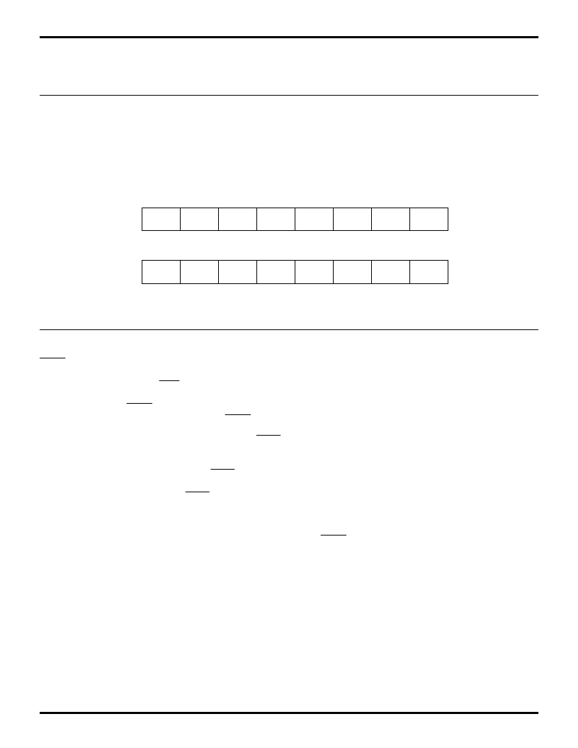
Figure 47. ASCI Extension Control Registers, Channel 0 and 1
Bit
DCDO
7
6
5
4
3
2
1
0
XI
BRGO
Mode
Break
Nab
Break
Send
Break
ASCI Extension Control Register 0(ASEXT0 I/O Address = 12H)
CTSO
Bit
7
6
5
4
3
2
1
0
XI
BRGI
Mode
Break
Enab
Break
Send
Break
ASCI Extension Control Register 1 (ASEXT1 I/O Address = 13H)
Reserved
Reserved Reserved Reserved
相關(guān)PDF資料 |
PDF描述 |
|---|---|
| Z8S18033VEC | CONN HDR INVERSE 30POS 5ROW R/A |
| Z8S18033VSC | CONN HDR INVERSE 120POS 5ROW R/A |
| Z8S180 | CAP 0.1UF 100V +80-20% Z5U AXIAL TR-14 |
| Z8S18006FEC | CAP 1UF 50V 10% X7R AXIAL TR-14 |
| Z8S18006FSC | CAP 0.47UF 50V 10% X7R AXIAL TR-14 |
相關(guān)代理商/技術(shù)參數(shù) |
參數(shù)描述 |
|---|---|
| Z8S18033VEC | 功能描述:微處理器 - MPU 33MHz STATIC Z180 XT RoHS:否 制造商:Atmel 處理器系列:SAMA5D31 核心:ARM Cortex A5 數(shù)據(jù)總線寬度:32 bit 最大時(shí)鐘頻率:536 MHz 程序存儲(chǔ)器大小:32 KB 數(shù)據(jù) RAM 大小:128 KB 接口類型:CAN, Ethernet, LIN, SPI,TWI, UART, USB 工作電源電壓:1.8 V to 3.3 V 最大工作溫度:+ 85 C 安裝風(fēng)格:SMD/SMT 封裝 / 箱體:FBGA-324 |
| Z8S18033VEC00TR | 功能描述:IC Z180 MPU 68PLCC RoHS:否 類別:集成電路 (IC) >> 嵌入式 - 微處理器 系列:Z180 標(biāo)準(zhǔn)包裝:40 系列:MPC83xx 處理器類型:32-位 MPC83xx PowerQUICC II Pro 特點(diǎn):- 速度:267MHz 電壓:0.95 V ~ 1.05 V 安裝類型:表面貼裝 封裝/外殼:516-BBGA 裸露焊盤 供應(yīng)商設(shè)備封裝:516-PBGAPGE(27x27) 包裝:托盤 |
| Z8S18033VEG | 功能描述:微處理器 - MPU 33MHz STATIC Z180 XT RoHS:否 制造商:Atmel 處理器系列:SAMA5D31 核心:ARM Cortex A5 數(shù)據(jù)總線寬度:32 bit 最大時(shí)鐘頻率:536 MHz 程序存儲(chǔ)器大小:32 KB 數(shù)據(jù) RAM 大小:128 KB 接口類型:CAN, Ethernet, LIN, SPI,TWI, UART, USB 工作電源電壓:1.8 V to 3.3 V 最大工作溫度:+ 85 C 安裝風(fēng)格:SMD/SMT 封裝 / 箱體:FBGA-324 |
| Z8S18033VSC | 功能描述:微處理器 - MPU 33MHz STATIC Z180 RoHS:否 制造商:Atmel 處理器系列:SAMA5D31 核心:ARM Cortex A5 數(shù)據(jù)總線寬度:32 bit 最大時(shí)鐘頻率:536 MHz 程序存儲(chǔ)器大小:32 KB 數(shù)據(jù) RAM 大小:128 KB 接口類型:CAN, Ethernet, LIN, SPI,TWI, UART, USB 工作電源電壓:1.8 V to 3.3 V 最大工作溫度:+ 85 C 安裝風(fēng)格:SMD/SMT 封裝 / 箱體:FBGA-324 |
| Z8S180-33VSC | 制造商:Zilog Inc 功能描述:IC CPU (Z80B) SMD 8S180 PLCC68 |
發(fā)布緊急采購(gòu),3分鐘左右您將得到回復(fù)。