- 您現(xiàn)在的位置:買(mǎi)賣(mài)IC網(wǎng) > PDF目錄371435 > 28F320D18 (Intel Corp.) 1.8 Volt Intel Dual-Plane Flash Memory(1.8 V Intel 雙平面閃速存儲(chǔ)器) PDF資料下載
參數(shù)資料
| 型號(hào): | 28F320D18 |
| 廠商: | Intel Corp. |
| 英文描述: | 1.8 Volt Intel Dual-Plane Flash Memory(1.8 V Intel 雙平面閃速存儲(chǔ)器) |
| 中文描述: | 1.8 V的英特爾雙平面閃存(1.8伏英特爾雙平面閃速存儲(chǔ)器) |
| 文件頁(yè)數(shù): | 18/83頁(yè) |
| 文件大小: | 836K |
| 代理商: | 28F320D18 |
第1頁(yè)第2頁(yè)第3頁(yè)第4頁(yè)第5頁(yè)第6頁(yè)第7頁(yè)第8頁(yè)第9頁(yè)第10頁(yè)第11頁(yè)第12頁(yè)第13頁(yè)第14頁(yè)第15頁(yè)第16頁(yè)第17頁(yè)當(dāng)前第18頁(yè)第19頁(yè)第20頁(yè)第21頁(yè)第22頁(yè)第23頁(yè)第24頁(yè)第25頁(yè)第26頁(yè)第27頁(yè)第28頁(yè)第29頁(yè)第30頁(yè)第31頁(yè)第32頁(yè)第33頁(yè)第34頁(yè)第35頁(yè)第36頁(yè)第37頁(yè)第38頁(yè)第39頁(yè)第40頁(yè)第41頁(yè)第42頁(yè)第43頁(yè)第44頁(yè)第45頁(yè)第46頁(yè)第47頁(yè)第48頁(yè)第49頁(yè)第50頁(yè)第51頁(yè)第52頁(yè)第53頁(yè)第54頁(yè)第55頁(yè)第56頁(yè)第57頁(yè)第58頁(yè)第59頁(yè)第60頁(yè)第61頁(yè)第62頁(yè)第63頁(yè)第64頁(yè)第65頁(yè)第66頁(yè)第67頁(yè)第68頁(yè)第69頁(yè)第70頁(yè)第71頁(yè)第72頁(yè)第73頁(yè)第74頁(yè)第75頁(yè)第76頁(yè)第77頁(yè)第78頁(yè)第79頁(yè)第80頁(yè)第81頁(yè)第82頁(yè)第83頁(yè)
28F320D18
14
Product Preview
3.3.1
Reading the Protection Register
The protection register is read by using the Read Device Identifier command (90H). Once in this
mode, read cycles from addresses shown in Appendix B retrieve the specified protection register
information. To return to read array mode, use the Read Array command (FFH).
3.3.2
Programming the Protection Register
The protection register bits are programmed using the two-cycle Protection Program command.
The 64-bit number is programmed 16 bits at a time. First write the Protection Program Setup
command, C0H. The next write to the device will latch in address and data to program the specified
location. The allowable addresses are shown in Appendix B. See
Figure 12, “Protection Register
Programming Flowchart” on page 30
.
Any attempt to address Protection Program commands outside the defined protection register
address space should not be performed. Attempting to program to a previously locked protection
register segment will result in a status register error (program error bit SR.4 and lock error bit
SR.1 = 1).
3.3.3
Locking the Protection Register
The customer-programmable segment of the protection register is lockable by programming Bit 1
of the PR-LOCK location to 0. Bit 0 of this location is programmed to 0 at the Intel factory to
protect the unique device number. This bit is set using the Protection Program command to
program “FFFD” to the PR-LOCK location. After these bits have been programmed, no further
changes can be made to the values stored in the protection register. Protection Program commands
to a locked section will result in a status register error program error bit SR.4 and lock error bit
SR.1 will be set to 1). Protection register lockout state is not reversible.
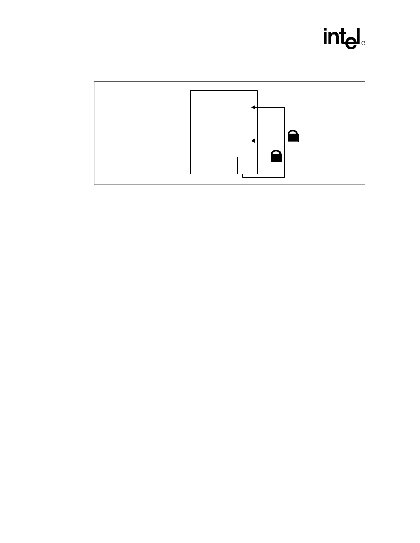
Figure 4. Protection Register Memory Map
4 Words
Intel Programmed
4 Words
Customer
Programmed
1 Word Lock
0088H
0085H
0084H
0081H
0080H
相關(guān)PDF資料 |
PDF描述 |
|---|---|
| 28F320J5 | 5 Volt Intel StrataFlash Memory(5 V 32M位英特爾StrataFlash存儲(chǔ)器) |
| 28F640J5 | 5 V Intel StrataFlash Memory(5V 64M位英特爾StrataFlash閃速存儲(chǔ)器) |
| 28F400B3 | SMART 3 ADVANCED BOOT BLOCK WORD-WIDE |
| 28F400BL-TB | 4-MBlT (256K x 16, 512K x 8) LOW-POWER BOOT BLOCK FLASH MEMORY FAMILY |
| 28F400BV-TB | 4-MBIT (256K X 16, 512K X 8)SmartVoltage BOOT BLOCK FLASH MEMORY FAMILY |
相關(guān)代理商/技術(shù)參數(shù) |
參數(shù)描述 |
|---|---|
| 28F320J3D75 | 制造商:undefined 功能描述: |
| 28F320J5 | 制造商:INTEL 制造商全稱(chēng):Intel Corporation 功能描述:StrataFlash MEMORY TECHNOLOGY 32 AND 64 MBIT |
| 28F320J5_02 | 制造商:INTEL 制造商全稱(chēng):Intel Corporation 功能描述:5 Volt Intel StrataFlash? Memory |
| 28F320S3 | 制造商:未知廠家 制造商全稱(chēng):未知廠家 功能描述:WORD-WIDE FlashFile MEMORY FAMILY |
| 28F320S5 | 制造商:未知廠家 制造商全稱(chēng):未知廠家 功能描述:WORD-WIDE FlashFile MEMORY FAMILY |
發(fā)布緊急采購(gòu),3分鐘左右您將得到回復(fù)。