- 您現在的位置:買賣IC網 > PDF目錄360546 > 79RC32V333-150DH 8 PIN, 1.75KB, FLASH, 64B RAM, COMPARATOR, 8MHZ INTERNAL OSCILLATOR, -40C to +125C, 8-PDIP, TUBE PDF資料下載
參數資料
| 型號: | 79RC32V333-150DH |
| 英文描述: | 8 PIN, 1.75KB, FLASH, 64B RAM, COMPARATOR, 8MHZ INTERNAL OSCILLATOR, -40C to +125C, 8-PDIP, TUBE |
| 中文描述: | 微處理器 |
| 文件頁數: | 540/654頁 |
| 文件大小: | 6963K |
| 代理商: | 79RC32V333-150DH |
第1頁第2頁第3頁第4頁第5頁第6頁第7頁第8頁第9頁第10頁第11頁第12頁第13頁第14頁第15頁第16頁第17頁第18頁第19頁第20頁第21頁第22頁第23頁第24頁第25頁第26頁第27頁第28頁第29頁第30頁第31頁第32頁第33頁第34頁第35頁第36頁第37頁第38頁第39頁第40頁第41頁第42頁第43頁第44頁第45頁第46頁第47頁第48頁第49頁第50頁第51頁第52頁第53頁第54頁第55頁第56頁第57頁第58頁第59頁第60頁第61頁第62頁第63頁第64頁第65頁第66頁第67頁第68頁第69頁第70頁第71頁第72頁第73頁第74頁第75頁第76頁第77頁第78頁第79頁第80頁第81頁第82頁第83頁第84頁第85頁第86頁第87頁第88頁第89頁第90頁第91頁第92頁第93頁第94頁第95頁第96頁第97頁第98頁第99頁第100頁第101頁第102頁第103頁第104頁第105頁第106頁第107頁第108頁第109頁第110頁第111頁第112頁第113頁第114頁第115頁第116頁第117頁第118頁第119頁第120頁第121頁第122頁第123頁第124頁第125頁第126頁第127頁第128頁第129頁第130頁第131頁第132頁第133頁第134頁第135頁第136頁第137頁第138頁第139頁第140頁第141頁第142頁第143頁第144頁第145頁第146頁第147頁第148頁第149頁第150頁第151頁第152頁第153頁第154頁第155頁第156頁第157頁第158頁第159頁第160頁第161頁第162頁第163頁第164頁第165頁第166頁第167頁第168頁第169頁第170頁第171頁第172頁第173頁第174頁第175頁第176頁第177頁第178頁第179頁第180頁第181頁第182頁第183頁第184頁第185頁第186頁第187頁第188頁第189頁第190頁第191頁第192頁第193頁第194頁第195頁第196頁第197頁第198頁第199頁第200頁第201頁第202頁第203頁第204頁第205頁第206頁第207頁第208頁第209頁第210頁第211頁第212頁第213頁第214頁第215頁第216頁第217頁第218頁第219頁第220頁第221頁第222頁第223頁第224頁第225頁第226頁第227頁第228頁第229頁第230頁第231頁第232頁第233頁第234頁第235頁第236頁第237頁第238頁第239頁第240頁第241頁第242頁第243頁第244頁第245頁第246頁第247頁第248頁第249頁第250頁第251頁第252頁第253頁第254頁第255頁第256頁第257頁第258頁第259頁第260頁第261頁第262頁第263頁第264頁第265頁第266頁第267頁第268頁第269頁第270頁第271頁第272頁第273頁第274頁第275頁第276頁第277頁第278頁第279頁第280頁第281頁第282頁第283頁第284頁第285頁第286頁第287頁第288頁第289頁第290頁第291頁第292頁第293頁第294頁第295頁第296頁第297頁第298頁第299頁第300頁第301頁第302頁第303頁第304頁第305頁第306頁第307頁第308頁第309頁第310頁第311頁第312頁第313頁第314頁第315頁第316頁第317頁第318頁第319頁第320頁第321頁第322頁第323頁第324頁第325頁第326頁第327頁第328頁第329頁第330頁第331頁第332頁第333頁第334頁第335頁第336頁第337頁第338頁第339頁第340頁第341頁第342頁第343頁第344頁第345頁第346頁第347頁第348頁第349頁第350頁第351頁第352頁第353頁第354頁第355頁第356頁第357頁第358頁第359頁第360頁第361頁第362頁第363頁第364頁第365頁第366頁第367頁第368頁第369頁第370頁第371頁第372頁第373頁第374頁第375頁第376頁第377頁第378頁第379頁第380頁第381頁第382頁第383頁第384頁第385頁第386頁第387頁第388頁第389頁第390頁第391頁第392頁第393頁第394頁第395頁第396頁第397頁第398頁第399頁第400頁第401頁第402頁第403頁第404頁第405頁第406頁第407頁第408頁第409頁第410頁第411頁第412頁第413頁第414頁第415頁第416頁第417頁第418頁第419頁第420頁第421頁第422頁第423頁第424頁第425頁第426頁第427頁第428頁第429頁第430頁第431頁第432頁第433頁第434頁第435頁第436頁第437頁第438頁第439頁第440頁第441頁第442頁第443頁第444頁第445頁第446頁第447頁第448頁第449頁第450頁第451頁第452頁第453頁第454頁第455頁第456頁第457頁第458頁第459頁第460頁第461頁第462頁第463頁第464頁第465頁第466頁第467頁第468頁第469頁第470頁第471頁第472頁第473頁第474頁第475頁第476頁第477頁第478頁第479頁第480頁第481頁第482頁第483頁第484頁第485頁第486頁第487頁第488頁第489頁第490頁第491頁第492頁第493頁第494頁第495頁第496頁第497頁第498頁第499頁第500頁第501頁第502頁第503頁第504頁第505頁第506頁第507頁第508頁第509頁第510頁第511頁第512頁第513頁第514頁第515頁第516頁第517頁第518頁第519頁第520頁第521頁第522頁第523頁第524頁第525頁第526頁第527頁第528頁第529頁第530頁第531頁第532頁第533頁第534頁第535頁第536頁第537頁第538頁第539頁當前第540頁第541頁第542頁第543頁第544頁第545頁第546頁第547頁第548頁第549頁第550頁第551頁第552頁第553頁第554頁第555頁第556頁第557頁第558頁第559頁第560頁第561頁第562頁第563頁第564頁第565頁第566頁第567頁第568頁第569頁第570頁第571頁第572頁第573頁第574頁第575頁第576頁第577頁第578頁第579頁第580頁第581頁第582頁第583頁第584頁第585頁第586頁第587頁第588頁第589頁第590頁第591頁第592頁第593頁第594頁第595頁第596頁第597頁第598頁第599頁第600頁第601頁第602頁第603頁第604頁第605頁第606頁第607頁第608頁第609頁第610頁第611頁第612頁第613頁第614頁第615頁第616頁第617頁第618頁第619頁第620頁第621頁第622頁第623頁第624頁第625頁第626頁第627頁第628頁第629頁第630頁第631頁第632頁第633頁第634頁第635頁第636頁第637頁第638頁第639頁第640頁第641頁第642頁第643頁第644頁第645頁第646頁第647頁第648頁第649頁第650頁第651頁第652頁第653頁第654頁
IDT EJTAG System
On-Chip Interfaces
79RC32438 User Reference Manual
20 - 74
November 4, 2002
Notes
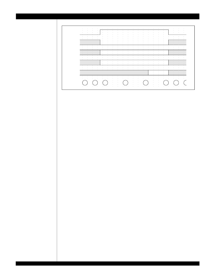
Figure 20.36 Read Processor Access Example
The different probe actions shown in the above figure are described below:
1. The EJTAG Control register is polled to get the indication for a pending PrAcc bit. The PrAcc bit is
written to 1 when polling, in order to prevent a processor access from finishing before being
serviced. The values of PRnW and Psz are saved when PrAcc indicates a pending processor
access.
2. The Address register is read. It contains the address of the load/fetch resulting in the write processor
access, with the three LSBs (64-bit processor) modified to allow size indication together with the
Psz.
3. The Data register is written with the data to return for the load/fetch, resulting in the read processor
access.
4. The PrAcc bit is cleared in order to finish the processor access.
The probe must provide data for the read processor access from the internal EJTAG memory. Note that
the Address register does not contain the direct address from the access, because the three LSBs (64-bit
processor) are modified to indicate the size in conjunction with Psz. Also notice that in this case, there is no
shifting of the data returned for the processor access by writing to the Data register, because a doubleword
is provided. For other accesses, the Data register must be written with a shifted value depending on the
specific access.
On-Chip Interfaces
Optional JTAG_TRST_N Pin
The JTAG_TRST_N signal to the TAP is optional, and need not be provided as a pin on the chip for a
processor implementing the EJTAG TAP. If a JTAG_TRST_N chip pin is not provided, then a TAP reset like
the one provided when JTAG_TRST_N is asserted (low) must be applied to the TAP at power-up, for
example, through a power-up reset circuit on the chip. This power-up TAP reset must be finished after the
time T
VIOrise
(see Figure 20.41). If a JTAG_TRST_N chip pin is provided, then the power-up TAP reset is
applied by a pull-down resistor, because the probe will not drive JTAG_TRST_N at power-up.
Input Buffers with Pull-Up/Down and Output Drivers for Chip Pins
If an input buffer with an integrated pull-up resistor is used for the JTAG_TRST_N chip pin, then its
resistor value must be sufficiently large that it is overruled by the external pull-down resistor on the PCB, so
a well-defined logical level is present on the JTAG_TRST_N pin (refer to section “Electrical Connection” on
page 20-81). Observe the additional rules described in the IEEE Std. 1149.1 specification, if the same TAP
PrAcc
Probe
action
PRnW
Psz
Address
Data
1
1
Address = = 0xF FF203457
Size = 3
2
3
4
1
1
0x0..0 Data =
相關PDF資料 |
PDF描述 |
|---|---|
| 79RC32V333-150DHI | Microprocessor |
| 79RC32V334-100BB | MICROPROCESSOR|32-BIT|BGA|256PIN|PLASTIC |
| 79RC32V334-100BBI | MICROPROCESSOR|32-BIT|BGA|256PIN|PLASTIC |
| 79RC32V334-133BB | MICROPROCESSOR|32-BIT|BGA|256PIN|PLASTIC |
| 79RC32V334-133BBI | MICROPROCESSOR|32-BIT|BGA|256PIN|PLASTIC |
相關代理商/技術參數 |
參數描述 |
|---|---|
| 79RC32V333-150DHI | 制造商:未知廠家 制造商全稱:未知廠家 功能描述:Microprocessor |
| 79RC32V334-100BB | 制造商:未知廠家 制造商全稱:未知廠家 功能描述:MICROPROCESSOR|32-BIT|BGA|256PIN|PLASTIC |
| 79RC32V334-100BBG | 制造商:Integrated Device Technology Inc 功能描述:MPU RC32300 32-Bit 100MHz 3.3V 256-Pin BGA |
| 79RC32V334-100BBGI | 制造商:Integrated Device Technology Inc 功能描述:MPU RC32300 32-Bit 100MHz 3.3V 256-Pin BGA |
| 79RC32V334-100BBI | 制造商:Integrated Device Technology Inc 功能描述:MPU RC32300 32-Bit 100MHz 3.3V 256-Pin BGA |
發(fā)布緊急采購,3分鐘左右您將得到回復。