- 您現(xiàn)在的位置:買賣IC網(wǎng) > PDF目錄378211 > 80960JS (Intel Corp.) High Performance 32-bit Embedded 3.3V Microprocessor(3.3V高性能32位嵌入式處理器) PDF資料下載
參數(shù)資料
| 型號(hào): | 80960JS |
| 廠商: | Intel Corp. |
| 英文描述: | High Performance 32-bit Embedded 3.3V Microprocessor(3.3V高性能32位嵌入式處理器) |
| 中文描述: | 高性能32位嵌入式微處理器3.3(3.3高性能32位嵌入式處理器) |
| 文件頁數(shù): | 21/86頁 |
| 文件大小: | 1257K |
| 代理商: | 80960JS |
第1頁第2頁第3頁第4頁第5頁第6頁第7頁第8頁第9頁第10頁第11頁第12頁第13頁第14頁第15頁第16頁第17頁第18頁第19頁第20頁當(dāng)前第21頁第22頁第23頁第24頁第25頁第26頁第27頁第28頁第29頁第30頁第31頁第32頁第33頁第34頁第35頁第36頁第37頁第38頁第39頁第40頁第41頁第42頁第43頁第44頁第45頁第46頁第47頁第48頁第49頁第50頁第51頁第52頁第53頁第54頁第55頁第56頁第57頁第58頁第59頁第60頁第61頁第62頁第63頁第64頁第65頁第66頁第67頁第68頁第69頁第70頁第71頁第72頁第73頁第74頁第75頁第76頁第77頁第78頁第79頁第80頁第81頁第82頁第83頁第84頁第85頁第86頁
80960JA/JF/JD/JS/JC/JT 3.3 V Microprocessor
Datasheet
21
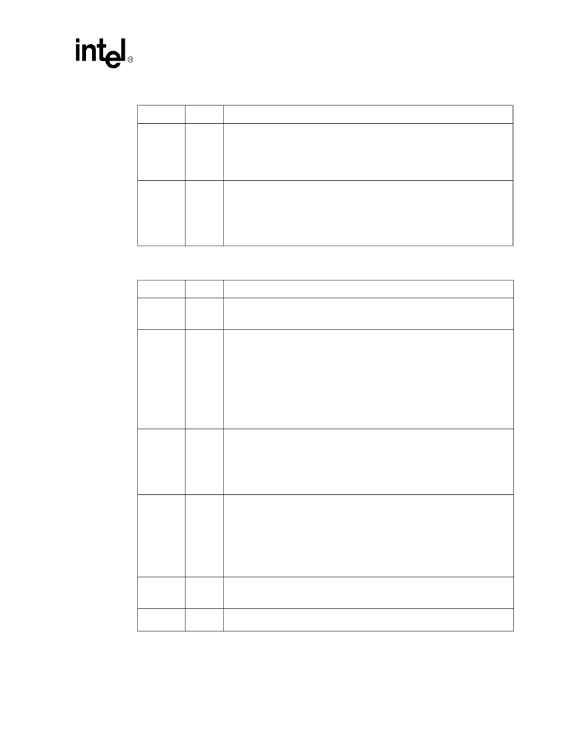
HOLDA
O
R(Q)
H(1)
P(Q)
HOLD ACKNOWLEDGE
indicates to an external bus master that the processor has
relinquished control of the bus. The processor can grant HOLD requests and enter
the T
h
state during reset and while halted as well as during regular operation.
0 = hold not acknowledged
1 = hold acknowledged
BSTAT
O
R(0)
H(Q)
P(0)
BUS STATUS
indicates that the processor may soon stall unless it has sufficient
access to the bus; see
i960
Jx
Microprocessor User
’
s Guide
(272483). Arbitration
logic can examine this signal to determine when an external bus master should
acquire/relinquish the bus.
0 = no potential stall
1 = potential stall
Table 9. Pin Description
—
Processor Control Signals, Test Signals and Power (Sheet 1 of 2)
NAME
TYPE
DESCRIPTION
CLKIN
I
CLOCK
INPUT
provides the processor
’
s fundamental time base; both the processor
core and the external bus run at the CLKIN rate. All input and output timings are
specified relative to a rising CLKIN edge.
RESET#
I
A(L)
RESET
initializes the processor and clears its internal logic. During reset, the
processor places the address/data bus and control output pins in their idle (inactive)
states.
During reset, the input pins are ignored with the exception of LOCK#/ONCE#,
STEST and HOLD.
The RESET# pin has an internal synchronizer. To ensure predictable processor
initialization during power up, RESET# must be asserted a minimum of 10,000
CLKIN cycles with V
and CLKIN stable. On a warm reset, RESET# should be
asserted for a minimum of 15 cycles.
STEST
I
S(L)
SELF TEST
enables or disables the processor
’
s internal self-test feature at
initialization. STEST is examined at the end of reset. When STEST is asserted, the
processor performs its internal self-test and the external bus confidence test. When
STEST is deasserted, the processor performs only the external bus confidence test.
0 = self test disabled
1 = self test enabled
FAIL#
O
R(0)
H(Q)
P(1)
FAIL
indicates a failure of the processor
’
s built-in self-test performed during
initialization. FAIL# is asserted immediately upon reset and toggles during self-test to
indicate the status of individual tests:
When self-test passes, the processor deasserts FAIL# and begins operation
from user code.
When self-test fails, the processor asserts FAIL# and then stops executing.
0 = self test failed
1 = self test passed
TCK
I
TEST CLOCK
is a CPU input which provides the clocking function for IEEE 1149.1
Boundary Scan Testing (JTAG). State information and data are clocked into the
processor on the rising edge; data is clocked out of the processor on the falling edge.
TDI
I
S(L)
TEST DATA INPUT
is the serial input pin for JTAG. TDI is sampled on the rising
edge of TCK, during the SHIFT-IR and SHIFT-DR states of the Test Access Port.
Table 8. Pin Description
—
External Bus Signals (Sheet 4 of 4)
NAME
TYPE
DESCRIPTION
相關(guān)PDF資料 |
PDF描述 |
|---|---|
| 80960JC | High Performance 32-Bit Embedded 3.3V Microprocessor(3.3V高性能32位嵌入式處理器) |
| 80960KB | Embedded 32-Bit Microprocessor With Integrated Floating-Point Unit(帶有集成的浮點(diǎn)單元的嵌入式32位微處理器) |
| 80960MC | Embedded 32Bit Microprocessor With Integrated Floating_Point Unit And Memory Unit(帶有集成的浮點(diǎn)單元和存儲(chǔ)器管理單元的嵌入式32位微處理器) |
| 80960RM | 80960RM I/O Processor(80960RM I/O 處理器) |
| 80960RN | 80960RN I/O Processor(80960RN I/O 處理器) |
相關(guān)代理商/技術(shù)參數(shù) |
參數(shù)描述 |
|---|---|
| 80960JT | 制造商:INTEL 制造商全稱:Intel Corporation 功能描述:3.3 V EMBEDDED 32-BIT MICROPROCESSOR |
| 80960KA | 制造商:INTEL 制造商全稱:Intel Corporation 功能描述:EMBEDDED 32-BIT MICROPROCESSOR |
| 80960KB | 制造商:INTEL 制造商全稱:Intel Corporation 功能描述:EMBEDDED 32-BIT MICROPROCESSOR WITH INTEGRATED FLOATING-POINT UNIT |
| 80960MC | 制造商:INTEL 制造商全稱:Intel Corporation 功能描述:EMBEDDED 32-BIT MICROPROCESSOR WITH INTEGRATED FLOATING-POINT UNIT AND MEMORY MANAGEMENT UNIT |
| 80960SA | 制造商:INTEL 制造商全稱:Intel Corporation 功能描述:EMBEDDED 32-BIT MICROPROCESSOR WITH 16-BIT BURST DATA BUS |
發(fā)布緊急采購,3分鐘左右您將得到回復(fù)。