- 您現(xiàn)在的位置:買賣IC網(wǎng) > PDF目錄378217 > 82845GV (INTEL CORP) Intel 82845G/82845GL/82845GV Graphics and Memory Controller Hub (GMCH) PDF資料下載
參數(shù)資料
| 型號(hào): | 82845GV |
| 廠商: | INTEL CORP |
| 元件分類: | 外設(shè)及接口 |
| 英文描述: | Intel 82845G/82845GL/82845GV Graphics and Memory Controller Hub (GMCH) |
| 中文描述: | MULTIFUNCTION PERIPHERAL, PBGA760 |
| 封裝: | 37.50 X 37.50 MM, 1 MM PITCH, FLIP CHIP, BGA-760 |
| 文件頁(yè)數(shù): | 25/193頁(yè) |
| 文件大小: | 2990K |
| 代理商: | 82845GV |
第1頁(yè)第2頁(yè)第3頁(yè)第4頁(yè)第5頁(yè)第6頁(yè)第7頁(yè)第8頁(yè)第9頁(yè)第10頁(yè)第11頁(yè)第12頁(yè)第13頁(yè)第14頁(yè)第15頁(yè)第16頁(yè)第17頁(yè)第18頁(yè)第19頁(yè)第20頁(yè)第21頁(yè)第22頁(yè)第23頁(yè)第24頁(yè)當(dāng)前第25頁(yè)第26頁(yè)第27頁(yè)第28頁(yè)第29頁(yè)第30頁(yè)第31頁(yè)第32頁(yè)第33頁(yè)第34頁(yè)第35頁(yè)第36頁(yè)第37頁(yè)第38頁(yè)第39頁(yè)第40頁(yè)第41頁(yè)第42頁(yè)第43頁(yè)第44頁(yè)第45頁(yè)第46頁(yè)第47頁(yè)第48頁(yè)第49頁(yè)第50頁(yè)第51頁(yè)第52頁(yè)第53頁(yè)第54頁(yè)第55頁(yè)第56頁(yè)第57頁(yè)第58頁(yè)第59頁(yè)第60頁(yè)第61頁(yè)第62頁(yè)第63頁(yè)第64頁(yè)第65頁(yè)第66頁(yè)第67頁(yè)第68頁(yè)第69頁(yè)第70頁(yè)第71頁(yè)第72頁(yè)第73頁(yè)第74頁(yè)第75頁(yè)第76頁(yè)第77頁(yè)第78頁(yè)第79頁(yè)第80頁(yè)第81頁(yè)第82頁(yè)第83頁(yè)第84頁(yè)第85頁(yè)第86頁(yè)第87頁(yè)第88頁(yè)第89頁(yè)第90頁(yè)第91頁(yè)第92頁(yè)第93頁(yè)第94頁(yè)第95頁(yè)第96頁(yè)第97頁(yè)第98頁(yè)第99頁(yè)第100頁(yè)第101頁(yè)第102頁(yè)第103頁(yè)第104頁(yè)第105頁(yè)第106頁(yè)第107頁(yè)第108頁(yè)第109頁(yè)第110頁(yè)第111頁(yè)第112頁(yè)第113頁(yè)第114頁(yè)第115頁(yè)第116頁(yè)第117頁(yè)第118頁(yè)第119頁(yè)第120頁(yè)第121頁(yè)第122頁(yè)第123頁(yè)第124頁(yè)第125頁(yè)第126頁(yè)第127頁(yè)第128頁(yè)第129頁(yè)第130頁(yè)第131頁(yè)第132頁(yè)第133頁(yè)第134頁(yè)第135頁(yè)第136頁(yè)第137頁(yè)第138頁(yè)第139頁(yè)第140頁(yè)第141頁(yè)第142頁(yè)第143頁(yè)第144頁(yè)第145頁(yè)第146頁(yè)第147頁(yè)第148頁(yè)第149頁(yè)第150頁(yè)第151頁(yè)第152頁(yè)第153頁(yè)第154頁(yè)第155頁(yè)第156頁(yè)第157頁(yè)第158頁(yè)第159頁(yè)第160頁(yè)第161頁(yè)第162頁(yè)第163頁(yè)第164頁(yè)第165頁(yè)第166頁(yè)第167頁(yè)第168頁(yè)第169頁(yè)第170頁(yè)第171頁(yè)第172頁(yè)第173頁(yè)第174頁(yè)第175頁(yè)第176頁(yè)第177頁(yè)第178頁(yè)第179頁(yè)第180頁(yè)第181頁(yè)第182頁(yè)第183頁(yè)第184頁(yè)第185頁(yè)第186頁(yè)第187頁(yè)第188頁(yè)第189頁(yè)第190頁(yè)第191頁(yè)第192頁(yè)第193頁(yè)
Intel
82845G/82845GL/82845GV GMCH Datasheet
25
Signal Description
2.2
Memory Interface
2.2.1
DDR SDRAM Interface
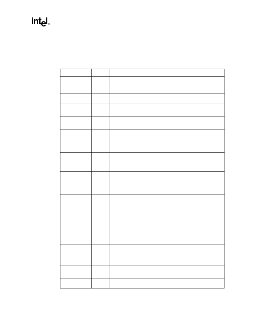
Signal Name
Type
Description
SCMDCLK_[5:0]
O
SSTL_2
Differential DDR Clock:
SCMDCLK and SCMDCLK# pairs are differential
clock outputs. The crossing of the positive edge of SCMDCLK and the
negative edge of SCMDCLK# is used to sample the address and control
signals on the SDRAM. There are 3 pairs to each DIMM.
SCMDCLK_[5:0]#
O
SSTL_2
Complementary Differential DDR Clock:
These are the complementary
Differential DDR Clock signals.
SCS_[3:0]#
O
SSTL_2
Chip Select:
These signals select particular SDRAM components during
the active state. There is one SCS# for each SDRAM row, toggled on the
positive edge of SCMDCLK.
SMAA_[12:0],
SMAB_[5,4,2,1]
O
SSTL_2
Memory Address:
These signals provide the multiplexed row and column
address to the SDRAM. SMAB_[5,4,2,1] signals are selective CPC signals
and are identical to SMAA_[5,4,2,1].
SBA[1:0]
O
SSTL_2
Bank Select (Bank Address):
These signals define which banks are
selected within each SDRAM row. Bank select and memory address signals
combine to address every possible location within an SDRAM device.
SRAS#
O
SSTL_2
Row Address Strobe:
SRAS# is used with SCAS# and SWE# (along with
SCS#) to define the SDRAM commands.
SCAS#
O
SSTL_2
Column Address Strobe:
SCAS# is used with SRAS# and SWE# (along
with SCS#) to define the SDRAM commands.
SWE#
O
SSTL_2
Write Enable:
SWE# is used with SCAS# and SRAS# (along with SCS#) to
define the SDRAM commands.
SDQ_[63:0]
I/O
SSTL_2
Data Lines:
SDQ_[63:0] interface to the SDRAM data bus.
SDM_[7:0]
O
SSTL_2
Data Mask:
When activated during writes, the corresponding data groups in
the SDRAM are masked. There is one SDM for every eight data lines. SDM
can be sampled on both edges of the data strobes.
SDQS_[7:0]
I/O
SSTL_2
Data Strobes:
Data strobes are used for capturing data. During writes,
SDQS is centered in data. During reads, SDQS is edge aligned with data.
The following list matches the data strobe with the data bytes.
SDQS_7 = SDQ_[63:56]
SDQS_6 = SDQ_[55:48]
SDQS_5 = SDQ_[47:40]
SDQS_4 = SDQ_[39:32]
SDQS_3 = SDQ_[31:24]
SDQS_2 = SDQ_[23:16]
SDQS_1 = SDQ_[15:8]
SDQS_0 = SDQ_[7:0]
SCKE_[3:0]
O
SSTL_2
Clock Enable:
SCKE is used to initialize DDR SDRAM during power-up and
to place all SDRAM rows into and out of self-refresh during Suspend-to-
RAM. SCKE is also used to dynamically power down inactive SDRAM rows.
There is one SCKE per SDRAM row, toggled on the positive edge of
SCMD_CLK.
SRCVEN_OUT#
O
SSTL_2
Receive Enable Out:
This signal is a feedback testpoint signal used to
enable the DQS input buffers during reads. This pin should be connect to
SRCVEN_IN through an
un-populated
backside resistor site.
SRCVEN_IN#
I
SSTL_2
Receive Enable In:
This signal is a feedback testpoint signal used to
enable the DQS input buffers during reads.
相關(guān)PDF資料 |
PDF描述 |
|---|---|
| 82845Gx | Intel 82845G/82845GL/82845GV Graphics and Memory Controller Hub (GMCH) |
| 82845MP | Intel 845 Family Chipset-Mobile 82845MP/82845MZ Chipset Memory Controller Hub Mobile (MCH-M) |
| 82845Mx | Intel 845 Family Chipset-Mobile 82845MP/82845MZ Chipset Memory Controller Hub Mobile (MCH-M) |
| 82845MZ | Intel 845 Family Chipset-Mobile 82845MP/82845MZ Chipset Memory Controller Hub Mobile (MCH-M) |
| 82845PE | 82845GE Graphics and Memory Controller Hub (GMCH) and 82845PE Memory Controller Hub (MCH) |
相關(guān)代理商/技術(shù)參數(shù) |
參數(shù)描述 |
|---|---|
| 82845GX | 制造商:INTEL 制造商全稱:Intel Corporation 功能描述:Intel 82845G/82845GL/82845GV Graphics and Memory Controller Hub (GMCH) |
| 82845MP | 制造商:INTEL 制造商全稱:Intel Corporation 功能描述:Intel 845 Family Chipset-Mobile 82845MP/82845MZ Chipset Memory Controller Hub Mobile (MCH-M) |
| 82845MX | 制造商:INTEL 制造商全稱:Intel Corporation 功能描述:Intel 845 Family Chipset-Mobile 82845MP/82845MZ Chipset Memory Controller Hub Mobile (MCH-M) |
| 82845MZ | 制造商:INTEL 制造商全稱:Intel Corporation 功能描述:Intel 845 Family Chipset-Mobile 82845MP/82845MZ Chipset Memory Controller Hub Mobile (MCH-M) |
| 82845PE | 制造商:INTEL 制造商全稱:Intel Corporation 功能描述:82845GE Graphics and Memory Controller Hub (GMCH) and 82845PE Memory Controller Hub (MCH) |
發(fā)布緊急采購(gòu),3分鐘左右您將得到回復(fù)。