- 您現(xiàn)在的位置:買賣IC網(wǎng) > PDF目錄373891 > AD6653BCPZ-125 (ANALOG DEVICES INC) IF Diversity Receiver PDF資料下載
參數(shù)資料
| 型號: | AD6653BCPZ-125 |
| 廠商: | ANALOG DEVICES INC |
| 元件分類: | 無繩電話/電話 |
| 英文描述: | IF Diversity Receiver |
| 中文描述: | TELECOM, CELLULAR, BASEBAND CIRCUIT, QCC64 |
| 封裝: | 9 X 9 MM, ROHS COMPLIANT, MO-220VMMD-4, LFCSP-64 |
| 文件頁數(shù): | 25/80頁 |
| 文件大?。?/td> | 1998K |
| 代理商: | AD6653BCPZ-125 |
第1頁第2頁第3頁第4頁第5頁第6頁第7頁第8頁第9頁第10頁第11頁第12頁第13頁第14頁第15頁第16頁第17頁第18頁第19頁第20頁第21頁第22頁第23頁第24頁當(dāng)前第25頁第26頁第27頁第28頁第29頁第30頁第31頁第32頁第33頁第34頁第35頁第36頁第37頁第38頁第39頁第40頁第41頁第42頁第43頁第44頁第45頁第46頁第47頁第48頁第49頁第50頁第51頁第52頁第53頁第54頁第55頁第56頁第57頁第58頁第59頁第60頁第61頁第62頁第63頁第64頁第65頁第66頁第67頁第68頁第69頁第70頁第71頁第72頁第73頁第74頁第75頁第76頁第77頁第78頁第79頁第80頁
AD6653
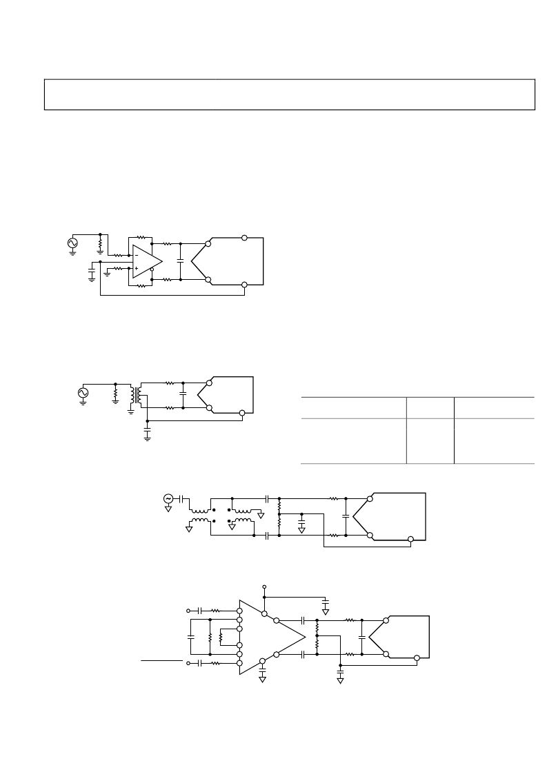
Differential Input Configurations
Optimum performance is achieved while driving the AD6653 in a
differential input configuration. For baseband applications, the
AD8138
,
ADA4937-2
, and
ADA4938-2
differential drivers provide
excellent performance and a flexible interface to the ADC. The
output common-mode voltage of the AD8138 is easily set with
the CML pin of the AD6653 (see Figure 47), and the driver can
be configured in a Sallen-Key filter topology to provide band
limiting of the input signal.
Rev. 0 | Page 25 of 80
AVDD
1V p-p
49.9
523
0.1μF
R
R
C
499
499
499
AD8138
AD6653
VIN+
VIN–
CML
0
Figure 47. Differential Input Configuration Using the AD8138
For baseband applications where SNR is a key parameter,
differential transformer coupling is the recommended input
configuration. An example is shown in Figure 48. To bias the
analog input, the CML voltage can be connected to the center
tap of the secondary winding of the transformer.
2V p-p
49.9
0.1μF
R
R
C
AD6653
VIN+
VIN–
CML
0
Figure 48. Differential Transformer-Coupled Configuration
The signal characteristics must be considered when selecting
a transformer. Most RF transformers saturate at frequencies
below a few megahertz (MHz). Excessive signal power can also
cause core saturation, which leads to distortion.
At input frequencies in the second Nyquist zone and above, the
noise performance of most amplifiers is not adequate to achieve
the true SNR performance of the AD6653. For applications where
SNR is a key parameter, differential double balun coupling is
the recommended input configuration (see Figure 49).
An alternative to using a transformer coupled input at frequencies
in the second Nyquist zone is to use the
AD8352
differential
driver, as shown in Figure 50. See the
AD8352
data sheet for
more information. In addition, if the application requires an
amplifier with variable gain, the
AD8375
or
AD8376
digital
variable gain amplifiers (DVGAs) provide good performance
driving the AD6653.
In any configuration, the value of the shunt capacitor, C, is
dependent on the input frequency and source impedance and
may need to be reduced or removed. Table 10 displays
recommended values to set the RC network. However, these
values are dependent on the input signal and should be used
only as a starting guide.
Table 10. Example RC Network
Frequency Range (MHz)
0 to 70
70 to 200
200 to 300
>300
R Series
(Ω Each)
33
33
15
15
C Differential (pF)
15
5
5
Open
AD6653
R
0.1μF
0.1μF
2V p-p
VIN+
VIN–
CML
C
R
0.1μF
S
0.1μF
25
25
S
P
A
P
0
Figure 49. Differential Double Balun Input Configuration
AD6653
AD8352
0
R
0
C
D
R
D
R
G
0.1μF
0.1μF
0.1μF
VIN+
VIN–
CML
C
0.1μF
16
1
2
3
4
5
11
R
0.1μF
0.1μF
10
14
0.1μF
8, 13
V
CC
200
200
ANALOG INPUT
ANALOG INPUT
0
Figure 50. Differential Input Configuration Using the AD8352
相關(guān)PDF資料 |
PDF描述 |
|---|---|
| AD6653BCPZ-150 | IF Diversity Receiver |
| AD6655BCPZ-1251 | IF Diversity Receiver |
| AD6655 | IF Diversity Receiver |
| AD6655-125EBZ1 | IF Diversity Receiver |
| AD6655-150EBZ1 | IF Diversity Receiver |
相關(guān)代理商/技術(shù)參數(shù) |
參數(shù)描述 |
|---|---|
| AD6653BCPZ-150 | 制造商:Analog Devices 功能描述:IF DIVERSITY RCVR 64LFCSP EP - Trays 制造商:Analog Devices 功能描述:IC RECEIVER IF DIVERSITY LFCSP64 制造商:Analog Devices 功能描述:IC, RECEIVER, IF DIVERSITY, LFCSP64 |
| AD6654 | 制造商:Analog Devices 功能描述:- Bulk |
| AD6654/PCB | 制造商:AD 制造商全稱:Analog Devices 功能描述:14-Bit, 92.16 MSPS, 4-/6-Channel Wideband IF to Baseband Receiver |
| AD6654/PCBZ | 制造商:Analog Devices 功能描述:4/6CH WIDEBAND IF TO BASEBAND RCVR - Bulk |
| AD6654BBC | 功能描述:IC ADC 14BIT W/6CH RSP 256CSPBGA RoHS:否 類別:集成電路 (IC) >> 數(shù)據(jù)采集 - 模數(shù)轉(zhuǎn)換器 系列:- 產(chǎn)品培訓(xùn)模塊:Lead (SnPb) Finish for COTS Obsolescence Mitigation Program 標(biāo)準(zhǔn)包裝:250 系列:- 位數(shù):12 采樣率(每秒):1.8M 數(shù)據(jù)接口:并聯(lián) 轉(zhuǎn)換器數(shù)目:1 功率耗散(最大):1.82W 電壓電源:模擬和數(shù)字 工作溫度:-40°C ~ 85°C 安裝類型:表面貼裝 封裝/外殼:48-LQFP 供應(yīng)商設(shè)備封裝:48-LQFP(7x7) 包裝:管件 輸入數(shù)目和類型:2 個單端,單極 |
發(fā)布緊急采購,3分鐘左右您將得到回復(fù)。