- 您現(xiàn)在的位置:買賣IC網(wǎng) > PDF目錄366891 > CR16MCS9VJE8 Microcontroller PDF資料下載
參數(shù)資料
| 型號: | CR16MCS9VJE8 |
| 英文描述: | Microcontroller |
| 中文描述: | 微控制器 |
| 文件頁數(shù): | 18/157頁 |
| 文件大?。?/td> | 1256K |
| 代理商: | CR16MCS9VJE8 |
第1頁第2頁第3頁第4頁第5頁第6頁第7頁第8頁第9頁第10頁第11頁第12頁第13頁第14頁第15頁第16頁第17頁當(dāng)前第18頁第19頁第20頁第21頁第22頁第23頁第24頁第25頁第26頁第27頁第28頁第29頁第30頁第31頁第32頁第33頁第34頁第35頁第36頁第37頁第38頁第39頁第40頁第41頁第42頁第43頁第44頁第45頁第46頁第47頁第48頁第49頁第50頁第51頁第52頁第53頁第54頁第55頁第56頁第57頁第58頁第59頁第60頁第61頁第62頁第63頁第64頁第65頁第66頁第67頁第68頁第69頁第70頁第71頁第72頁第73頁第74頁第75頁第76頁第77頁第78頁第79頁第80頁第81頁第82頁第83頁第84頁第85頁第86頁第87頁第88頁第89頁第90頁第91頁第92頁第93頁第94頁第95頁第96頁第97頁第98頁第99頁第100頁第101頁第102頁第103頁第104頁第105頁第106頁第107頁第108頁第109頁第110頁第111頁第112頁第113頁第114頁第115頁第116頁第117頁第118頁第119頁第120頁第121頁第122頁第123頁第124頁第125頁第126頁第127頁第128頁第129頁第130頁第131頁第132頁第133頁第134頁第135頁第136頁第137頁第138頁第139頁第140頁第141頁第142頁第143頁第144頁第145頁第146頁第147頁第148頁第149頁第150頁第151頁第152頁第153頁第154頁第155頁第156頁第157頁

www.national.com
18
8.0
Bus Interface Unit
The Bus Interface Unit (BIU) controls the interface between
the internal core bus and those on-chip modules which are
mapped into BIU zones. These on-chip modules are the flash
EEPROM program memory, the ISP-memory and the I/O-
zone. It determines the configured parameters for bus ac-
cess (such as the number of wait states for memory access)
and issues the appropriate bus signals for the requested ac-
cess.
Note:
The device is manufactured in a 224-pin version which
is used in emulation equipment. In the 224-pin device, the
BIU controls access to both on-chip and off-chip memory and
peripherals. Operation of the 224-pin device and the use of
chip-external memory is beyond the scope of this data sheet.
8.1
There are four types of data transfer bus cycles:
— Normal read
— Fast read
— Early write
— Late write
The type of data cycle used in a particular transaction de-
pends on the type of CPU operation (a write or a read), the
type of memory or I/O being accessed, and the access type
programmed into the BIU control registers (early/late write or
normal/fast read).
For read operations, a basic normal read takes two clock cy-
cles, whereas a fast read bus cycle takes one clock cycle.
Upon reset of the device, normal read bus cycles are enabled
by default.
For write operations, a basic late write bus cycle takes two
clock cycles, whereas a basic early write bus cycle takes
three clock cycles. Upon reset of the device, early write bus
cycles are enabled by default. However, late write bus cycles
are needed for ordinary write operations, so this configura-
tion should be changed by the application software (see
Section 8.2.1).
In certain cases, one or more additional clock cycles are add-
ed to a bus access cycle. There are two types of additional
clock cycles for ordinary memory accesses, called internal
wait cycles (TIW) and hold (Thold) cycles.
A wait cycle is inserted in a bus cycle just after the memory
address has been placed on the address bus. This gives the
accessed memory more time to respond to the transaction
request. A hold cycle is inserted at the end of a bus cycle.
This holds the data on the data bus for an extended number
of clock cycles.
BUS CYCLES
8.2
The BIU has a set of control registers that determine how
many wait cycles and hold cycles are to be used for access-
ing memory. Upon start-up of the device, these registers
should be programmed with appropriate values so that the
minimum allowable number of cycles is used. This number
varies with the clock frequency used.
There are four applicable BIU registers: the BIU Configura-
tion (BCFG) register, the I/O Configuration (IOCFG) register,
the Static Zone 0 Configuration (SZCFG0) register and the
Static Zone 1Configuration (SZCFG1) register. These regis-
ters control the bus cycle configuration used for accessing
the various on-chip memory types.
Note:
A system configuration register called the Module
Configuration (MCFG) register controls the number of wait
cycles used for accessing the EEPROM data memory. This
register is described in Section 5.1.
BIU CONTROL REGISTERS
8.2.1
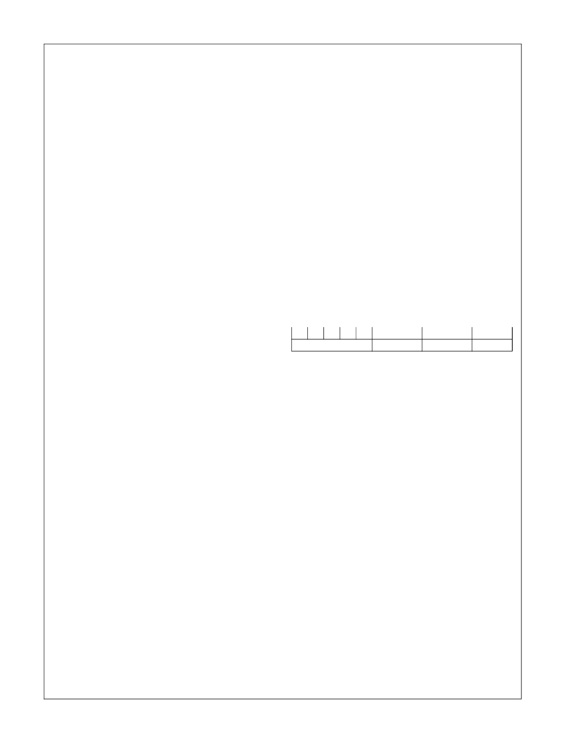
The BIU Configuration (BCFG) Register is a byte-wide, read/
write register that selects either early write or late write bus
cycles. The register address is F900 hex. Upon reset, the
register is initialized to 07 hex. The register format is shown
below.
7
6
5
4
3
2
Reserved
Note 1
BIU Configuration (BCFG) Register
EWR
Early Write. This bit is cleared to 0 for late write
operation (two clock cycles to write) or set to 1
for early write operation.
Note 1:
These bits (bit 1 or bit 2) control the configuration of
the 224-pin device used in emulation equipment. The CPU
should set this bit to 1 when it writes to the register.
Upon reset, the BCFG register is initialized to 07 hex, which
selects early write operation. However, late write operation is
required for normal device operation, so the software should
change the register value to 06 hex.
8.2.2
The I/O Zone Configuration (IOCFG) register is a word-wide,
read/write register that sets the timing and bus characteris-
tics of I/O Zone memory accesses. In the device implemen-
tation, the registers associated to Port B and Port C reside in
the I/O memory array. (These ports are used as a 16-bit data
port, if the device operates in development mode.)
I/O Zone Configuration (IOCFG) Register
1
0
Note 1
EWR
相關(guān)PDF資料 |
PDF描述 |
|---|---|
| CR16MCS9VJE8Y | Microcontroller |
| CR16MCT5VJE7Y | Microcontroller |
| CR16HCS5VJE8 | Microcontroller |
| CR16HCS9VJE7Y | Microcontroller |
| CR16HCS9VJE8Y | Microcontroller |
相關(guān)代理商/技術(shù)參數(shù) |
參數(shù)描述 |
|---|---|
| CR16MCS9VJE8/NOPB | 功能描述:16位微控制器 - MCU RoHS:否 制造商:Texas Instruments 核心:RISC 處理器系列:MSP430FR572x 數(shù)據(jù)總線寬度:16 bit 最大時鐘頻率:24 MHz 程序存儲器大小:8 KB 數(shù)據(jù) RAM 大小:1 KB 片上 ADC:Yes 工作電源電壓:2 V to 3.6 V 工作溫度范圍:- 40 C to + 85 C 封裝 / 箱體:VQFN-40 安裝風(fēng)格:SMD/SMT |
| CR16MCS9VJE80 | 制造商:NSC 制造商全稱:National Semiconductor 功能描述:Family of 16-bit CAN-enabled CompactRISC Microcontrollers |
| CR16MCS9VJE81 | 制造商:NSC 制造商全稱:National Semiconductor 功能描述:Family of 16-bit CAN-enabled CompactRISC Microcontrollers |
| CR16MCS9VJE82 | 制造商:NSC 制造商全稱:National Semiconductor 功能描述:Family of 16-bit CAN-enabled CompactRISC Microcontrollers |
| CR16MCS9VJE83 | 制造商:NSC 制造商全稱:National Semiconductor 功能描述:Family of 16-bit CAN-enabled CompactRISC Microcontrollers |
發(fā)布緊急采購,3分鐘左右您將得到回復(fù)。