- 您現(xiàn)在的位置:買賣IC網(wǎng) > PDF目錄366891 > CR16MCS9VJE8 Microcontroller PDF資料下載
參數(shù)資料
| 型號: | CR16MCS9VJE8 |
| 英文描述: | Microcontroller |
| 中文描述: | 微控制器 |
| 文件頁數(shù): | 79/157頁 |
| 文件大小: | 1256K |
| 代理商: | CR16MCS9VJE8 |
第1頁第2頁第3頁第4頁第5頁第6頁第7頁第8頁第9頁第10頁第11頁第12頁第13頁第14頁第15頁第16頁第17頁第18頁第19頁第20頁第21頁第22頁第23頁第24頁第25頁第26頁第27頁第28頁第29頁第30頁第31頁第32頁第33頁第34頁第35頁第36頁第37頁第38頁第39頁第40頁第41頁第42頁第43頁第44頁第45頁第46頁第47頁第48頁第49頁第50頁第51頁第52頁第53頁第54頁第55頁第56頁第57頁第58頁第59頁第60頁第61頁第62頁第63頁第64頁第65頁第66頁第67頁第68頁第69頁第70頁第71頁第72頁第73頁第74頁第75頁第76頁第77頁第78頁當(dāng)前第79頁第80頁第81頁第82頁第83頁第84頁第85頁第86頁第87頁第88頁第89頁第90頁第91頁第92頁第93頁第94頁第95頁第96頁第97頁第98頁第99頁第100頁第101頁第102頁第103頁第104頁第105頁第106頁第107頁第108頁第109頁第110頁第111頁第112頁第113頁第114頁第115頁第116頁第117頁第118頁第119頁第120頁第121頁第122頁第123頁第124頁第125頁第126頁第127頁第128頁第129頁第130頁第131頁第132頁第133頁第134頁第135頁第136頁第137頁第138頁第139頁第140頁第141頁第142頁第143頁第144頁第145頁第146頁第147頁第148頁第149頁第150頁第151頁第152頁第153頁第154頁第155頁第156頁第157頁

79
www.national.com
Acknowledge Cycle
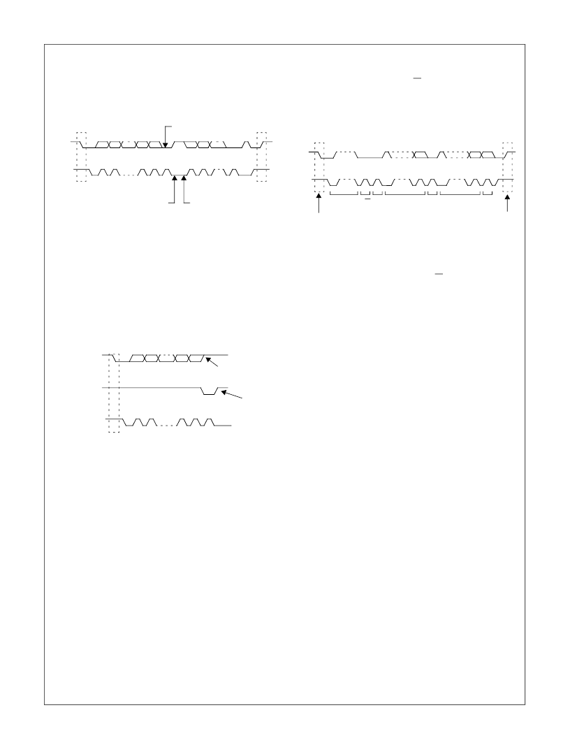
The Acknowledge Cycle consists of two signals: the ac-
knowledge clock pulse the master sends with each byte
transferred, and the acknowledge signal sent by the receiv-
ing device (Figure 41).
Figure 41.
ACCESS.bus Data Transaction
The master generates the acknowledge clock pulse on the
ninth clock pulse of the byte transfer. The transmitter releas-
es the SDA line (permits it to go high) to allow the receiver to
send the acknowledge signal. The receiver must pull down
the SDA line during the acknowledge clock pulse, thus sig-
nalling the correct reception of the last data byte, and its
readiness to receive the next byte. Figure 42 illustrates the
acknowledge cycle.
Figure 42.
ACCESS.bus Acknowledge Cycle
The master generates an acknowledge clock pulse after
each byte transfer. The receiver sends an acknowledge sig-
nal after every byte received.
There are two exceptions to the “acknowledge after every
byte” rule.
1. When the master is the receiver, it must indicate to the
transmitter an end of data by not-acknowledging (“neg-
ative acknowledge”) the last byte clocked out of the
slave. This “negative acknowledge” still includes the ac-
knowledge clock pulse (generated by the master), but
the SDA line is not pulled down.
2. When the receiver is full, otherwise occupied, or a prob-
lem has occurred, it sends a negative acknowledge to
indicate that it can not accept additional data bytes.
Addressing Transfer Formats
Each device on the bus has a unique address. Before any
data is transmitted, the master transmits the address of the
slave being addressed. The slave device should send an ac-
knowledge signal on the SDA line, once it recognizes its ad-
dress.
The address is the first seven bits after a Start Condition. The
direction of the data transfer (R/W) depends on the bit sent
after the address — the eighth bit. A low-to-high transition
during a SCL high period indicates the Stop Condition, and
ends the transaction (Figure 43).
Figure 43.
A Complete ACCESS.bus Data Transaction
When the address is sent, each device in the system com-
pares this address with its own. If there is a match, the device
considers itself addressed and sends an acknowledge sig-
nal. Depending upon the state of the R/W bit (1:read, 0:write),
the device acts as a transmitter or a receiver.
The I
2
C bus protocol allows sending a general call address
to all slaves connected to the bus. The first byte sent speci-
fies the general call address (00
16
) and the second byte
specifies the meaning of the general call (for example, “Write
slave address by software only”). Those slaves that require
the data acknowledge the call and become slave receivers;
the other slaves ignore the call.
Arbitration on the Bus
Multiple master devices on the bus, require arbitration be-
tween their conflicting bus-access demands. Control of the
bus is initially determined according to address bits and clock
cycle. If the masters are trying to address the same IC, data
comparisons determine the outcome of this arbitration. In
master mode, the device immediately aborts a transaction if
the value sampled on the SDA lines differs from the value
driven by the device. (Exceptions to this rule are SDA while
receiving data; in these cases the lines may be driven low by
the slave without causing an abort).
The SCL signal is monitored for clock synchronization pur-
pose and allow the slave to stall the bus. The actual clock pe-
riod will be the one set by the master with the longest clock
period or by the slave stall period. The clock high period is
determined by the master with the shortest clock high period.
When an abort occurs during the address transmission, the
master that identify the conflict, give-up the bus and should
switch to slave mode and continue to sample SDA to see if it
is being addressed by the winning master on the AC-
CESS.bus.
19.2
The ACB module provides the physical layer for an AC-
CESS.bus compliant serial interface. The module is config-
urable as either a master or slave device. As a slave device,
the ACB module may issue a request to become the bus
master.
ACB FUNCTIONAL DESCRIPTION
S
P
Start
Condition
Stop
Condition
SDA
SCL
MSB
ACK
ACK
1
2 3 - 6
7
8
9
1
2
3 - 8
9
Acknowledgment
Signal From Receiver
Byte Complete
I
nterrupt Within
Receiver
Clock Line Held
Low by Receiver
While Interrupt
is Serviced
S
Start
Condition
SCL
1
2 3 - 6
7
8
9
Transmitter Stays Off
the Bus During the
Acknowledgment Clock
Acknowledgment
Signal From Receiver
Data Output
by
Transmitter
Data Output
by
Receiver
S
P
Start
Condition
Stop
Condition
SDA
SCL
1 - 7
8
9
1 - 7
8
9
1 - 7
8
9
Address R/W ACK
Data
ACK
Data
ACK
相關(guān)PDF資料 |
PDF描述 |
|---|---|
| CR16MCS9VJE8Y | Microcontroller |
| CR16MCT5VJE7Y | Microcontroller |
| CR16HCS5VJE8 | Microcontroller |
| CR16HCS9VJE7Y | Microcontroller |
| CR16HCS9VJE8Y | Microcontroller |
相關(guān)代理商/技術(shù)參數(shù) |
參數(shù)描述 |
|---|---|
| CR16MCS9VJE8/NOPB | 功能描述:16位微控制器 - MCU RoHS:否 制造商:Texas Instruments 核心:RISC 處理器系列:MSP430FR572x 數(shù)據(jù)總線寬度:16 bit 最大時鐘頻率:24 MHz 程序存儲器大小:8 KB 數(shù)據(jù) RAM 大小:1 KB 片上 ADC:Yes 工作電源電壓:2 V to 3.6 V 工作溫度范圍:- 40 C to + 85 C 封裝 / 箱體:VQFN-40 安裝風(fēng)格:SMD/SMT |
| CR16MCS9VJE80 | 制造商:NSC 制造商全稱:National Semiconductor 功能描述:Family of 16-bit CAN-enabled CompactRISC Microcontrollers |
| CR16MCS9VJE81 | 制造商:NSC 制造商全稱:National Semiconductor 功能描述:Family of 16-bit CAN-enabled CompactRISC Microcontrollers |
| CR16MCS9VJE82 | 制造商:NSC 制造商全稱:National Semiconductor 功能描述:Family of 16-bit CAN-enabled CompactRISC Microcontrollers |
| CR16MCS9VJE83 | 制造商:NSC 制造商全稱:National Semiconductor 功能描述:Family of 16-bit CAN-enabled CompactRISC Microcontrollers |
發(fā)布緊急采購,3分鐘左右您將得到回復(fù)。