- 您現(xiàn)在的位置:買賣IC網(wǎng) > PDF目錄298975 > CY7C1009-15PC (CYPRESS SEMICONDUCTOR CORP) 128K X 8 STANDARD SRAM, 15 ns, PDIP32 PDF資料下載
參數(shù)資料
| 型號: | CY7C1009-15PC |
| 廠商: | CYPRESS SEMICONDUCTOR CORP |
| 元件分類: | SRAM |
| 英文描述: | 128K X 8 STANDARD SRAM, 15 ns, PDIP32 |
| 封裝: | 0.300 INCH, PLASTIC, DIP-32 |
| 文件頁數(shù): | 1/10頁 |
| 文件大小: | 245K |
| 代理商: | CY7C1009-15PC |
128K x 8 Static RAM
CY7C1009
PRELIMINARY
Cypress Semiconductor Corporation
3901 North First Street
San Jose
CA 95134
408-943-2600
December 1991 – Revised September 1996
1CY 7C10 09
Features
High speed
—tAA = 12 ns
CMOS for optimum speed/power
Low active power
— 1020 mW
Low standby power
—250 mW
2.0V data retention (optional)
— 100
W
Available in 450 x 550-mil LCC
Automatic power-down when deselected
Easy memory expansion with CE1, CE2, and OE options
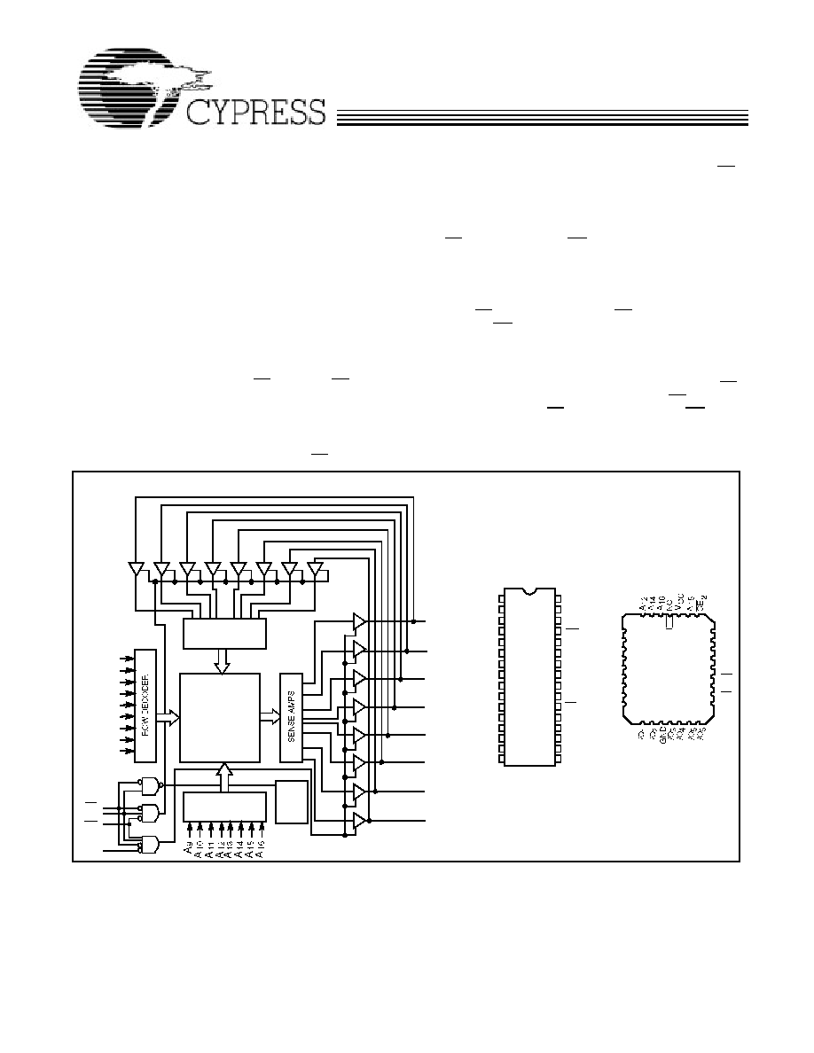
Functional Description
The CY7C1009 is a high-performance CMOS static RAM or-
ganized as 131,072 words by 8 bits. Easy memory expansion
is provided by an active LOW chip enable (CE1), an active
HIGH chip enable (CE2), an active LOW output enable (OE),
and three-state drivers. This device has an automatic pow-
er-down feature that reduces power consumption by more
than 75% when deselected.
Writing to the device is accomplished by taking chip enable
one (CE1) and write enable (WE) inputs LOW and chip enable
two (CE2) input HIGH. Data on the eight I/O pins (I/O0 through
I/O7) is then written into the location specified on the address
pins (A0 through A16).
Reading from the device is accomplished by taking chip en-
able one (CE1) and output enable (OE) LOW while forcing
write enable (WE) and chip enable two (CE2) HIGH. Under
these conditions, the contents of the memory location speci-
fied by the address pins will appear on the I/O pins.
The eight input/output pins (I/O0 through I/O7) are placed in a
high-impedance state when the device is deselected (CE1
HIGH or CE2 LOW), the outputs are disabled (OE HIGH), or
during a write operation (CE1 LOW, CE2 HIGH, and WE LOW).
The CY7C1009 is available in standard 300-mil-wide DIPs,
SOJs and a small footprint 450 x 550-mil leadless chip carrier.
Logic Block Diagram
Pin Configurations
A1
A2
A3
A4
A5
A6
A7
A8
COLUMN
DECODER
INPUT BUFFER
POWER
DOWN
WE
OE
I/O0
CE2
I/O1
I/O2
I/O3
512 x 256 x 8
ARRAY
I/O7
I/O6
I/O5
I/O4
A0
CE1
1
2
3
4
5
6
7
8
9
10
11
14
19
20
24
23
22
21
25
28
27
26
Top View
DIP/SOJ
12
13
29
32
31
30
16
15
17
18
GND
A16
A14
A12
A7
A6
A5
A4
A3
WE
VCC
A15
A13
A8
A9
I/O7
I/O6
I/O5
I/O4
A2
NC
I/O0
I/O1
I/O2
CE1
OE
A10
I/O3
A1
A0
A11
CE2
1009–1
1009–2
12
I/O0
31
4
5
6
7
8
9
10
32 1
30
13
14 15 16 17
26
25
24
23
22
21
11
A7
A6
A5
A4
A3
A2
A1
A10
A13
A8
A9
OE
CE1
I/O7
Top View
LCC
WE
A11
1819 20
27
28
29
32
1009–3
A0
相關(guān)PDF資料 |
PDF描述 |
|---|---|
| CY7C1016-15VCT | 256K X 4 STANDARD SRAM, 15 ns, PDSO32 |
| CY7C1020CV33-10ZXCT | 32K X 16 STANDARD SRAM, 10 ns, PDSO44 |
| CY7C1328F-133AC | 256K X 18 CACHE SRAM, 4 ns, PQFP100 |
| CY7C1339B-133BGIT | 128K X 32 CACHE SRAM, 4 ns, PBGA119 |
| CY7C1339G-200AXCT | 128K X 32 CACHE SRAM, 2.8 ns, PQFP100 |
相關(guān)代理商/技術(shù)參數(shù) |
參數(shù)描述 |
|---|---|
| CY7C100915V | 制造商:Cypress Semiconductor 功能描述: |
| CY7C100915VC | 制造商:Cypress Semiconductor 功能描述: |
| CY7C1009-15VC | 制造商:Cypress Semiconductor 功能描述:Static RAM, 128Kx8, 32 Pin, Plastic, SOJ |
| CY7C100915VIT | 制造商:CYPRESS 功能描述:* |
| CY7C1009-20LMB | 制造商:Cypress Semiconductor 功能描述:SRAM Chip Async Single 5V 1M-Bit 128K x 8 20ns 32-Pin LCC |
發(fā)布緊急采購,3分鐘左右您將得到回復(fù)。