- 您現(xiàn)在的位置:買賣IC網(wǎng) > PDF目錄298975 > CY7C1339B-133BGIT (CYPRESS SEMICONDUCTOR CORP) 128K X 32 CACHE SRAM, 4 ns, PBGA119 PDF資料下載
參數(shù)資料
| 型號: | CY7C1339B-133BGIT |
| 廠商: | CYPRESS SEMICONDUCTOR CORP |
| 元件分類: | SRAM |
| 英文描述: | 128K X 32 CACHE SRAM, 4 ns, PBGA119 |
| 封裝: | 14 X 22 MM, 2.40 MM HEIGHT, PLASTIC, BGA-119 |
| 文件頁數(shù): | 1/17頁 |
| 文件大小: | 527K |
| 代理商: | CY7C1339B-133BGIT |
128K x 32 Synchronous Pipelined Cache RAM
CY7C1339B
Cypress Semiconductor Corporation
3901 North First Street
San Jose
CA 95134
408-943-2600
Document #: 38-05141 Rev. *A
Revised March 27, 2002
Features
Supports 100-MHz bus for Pentium
and PowerPC
operations with zero wait states
Fully registered inputs and outputs for pipelined
operation
128K × 32 common I/O architecture
3.3V core power supply
2.5V / 3.3V I/O operation
Fast clock-to-output times
— 3.5 ns (for 166-MHz device)
— 4.0 ns (for 133-MHz device)
— 5.5 ns (for 100-MHz device)
User-selectable burst counter supporting Intel
Pentium interleaved or linear burst sequences
Separate processor and controller address strobes
Synchronous self-timed writes
Asynchronous output enable
Offered in JEDEC-standard 100-pin TQFP and 119-ball
BGA packages
“ZZ” Sleep Mode and Stop Clock options
Functional Description
The CY7C1339B is a 3.3V, 128K by 32 synchronous-pipelined
cache SRAM designed to support zero wait state secondary
cache with minimal glue logic.
The CY7C1339B I/O pins can operate at either the 2.5V or the
3.3V level; the I/O pins are 3.3V-tolerant when VDDQ = 2.5V.
All synchronous inputs pass through input registers controlled
by the rising edge of the clock. All data outputs pass through
output registers controlled by the rising edge of the clock.
Maximum access delay from the clock rise is 3.5 ns (166-MHz
device).
The CY7C1339B supports either the interleaved burst
sequence used by the Intel Pentium processor or a linear burst
sequence used by processors such as the PowerPC. The
burst sequence is selected through the MODE pin. Accesses
can be initiated by asserting either the Processor Address
Strobe (ADSP) or the Controller Address Strobe (ADSC) at
clock rise. Address advancement through the burst sequence
is controlled by the ADV input. A two-bit on-chip wraparound
burst counter captures the first address in a burst sequence
and automatically increments the address for the rest of the
burst access.
Byte Write operations are qualified with the four Byte Write
Select (BW[3:0]) inputs. A Global Write Enable (GW) overrides
all Byte Write inputs and writes data to all four bytes. All Writes
are conducted with on-chip synchronous self-timed Write
circuitry.
Three synchronous Chip Selects (CE1, CE2, CE3) and an
asynchronous Output Enable (OE) provide for easy bank
selection and output three-state control. In order to provide
proper data during depth expansion, OE is masked during the
first clock of a Read cycle when emerging from a deselected
state.
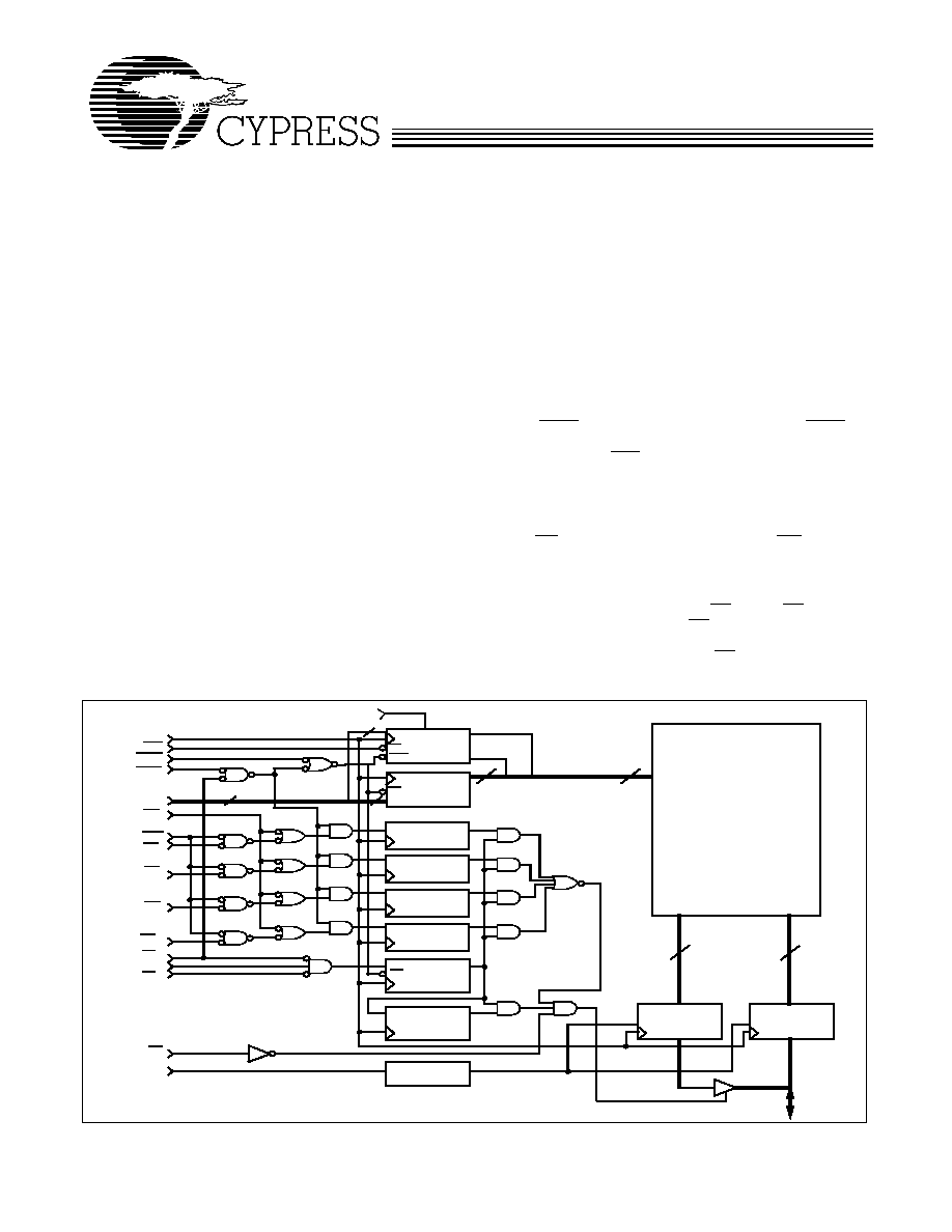
CLK
ADV
ADSC
A[16:0]
GW
BWE
BW 3
BW
2
BW1
BW0
CE1
CE3
CE2
OE
ZZ
BURST
COUNTER
DQ[31:24]
BYTEWRITE
REGISTERS
ADDRESS
REGISTER
D
Q
OUTPUT
REGISTERS
INPUT
REGISTERS
128K × 32
MEMORY
ARRAY
CLK
Q0
Q1
Q
D
CE
CLR
SLEEP
CONTROL
DQ[23:16]
BYTEWRITE
REGISTERS
D
Q
DQ
DQ[15:8]
BYTEWRITE
REGISTERS
DQ[7:0]
BYTEWRITE
REGISTERS
D
Q
ENABLE
REGISTER
D
Q
CE
CLK
ENABLE DELAY
REGISTER
D
Q
CLK
32
17
15
17
(A[1;0])
2
MODE
ADSP
Logic Block Diagram
DQ[31:0]
相關PDF資料 |
PDF描述 |
|---|---|
| CY7C1339G-200AXCT | 128K X 32 CACHE SRAM, 2.8 ns, PQFP100 |
| CY7C1347D-250BGC | 128K X 36 CACHE SRAM, 2.4 ns, PBGA119 |
| CY7C1512JV18-267BZXC | 4M X 18 QDR SRAM, 0.45 ns, PBGA165 |
| CY7C1515AV18-250BZXI | 2M X 36 QDR SRAM, 0.45 ns, PBGA165 |
| CY7C1522JV18-250BZI | 8M X 8 DDR SRAM, 0.45 ns, PBGA165 |
相關代理商/技術參數(shù) |
參數(shù)描述 |
|---|---|
| CY7C1339F-100AC | 制造商:Cypress Semiconductor 功能描述:SRAM Chip Sync Single 3.3V 4M-Bit 128K x 32 4.5ns 100-Pin TQFP |
| CY7C1339F-100BGI | 制造商:Cypress Semiconductor 功能描述: |
| CY7C1339F-100BGIT | 制造商:Cypress Semiconductor 功能描述:SRAM Chip Sync Single 3.3V 4M-Bit 128K x 32 4.5ns 119-Pin BGA T/R |
| CY7C1339F-133AC | 制造商:Cypress Semiconductor 功能描述:SRAM Chip Sync Single 3.3V 4M-Bit 128K x 32 4ns 100-Pin TQFP |
| CY7C1339F-166AC | 制造商:Rochester Electronics LLC 功能描述:128KX32 3.3V SYNC-PL SRAM (2.5/3.3V I/O) 1CD - Bulk |
發(fā)布緊急采購,3分鐘左右您將得到回復。