- 您現(xiàn)在的位置:買賣IC網(wǎng) > PDF目錄298975 > CY7C1339G-200AXCT (CYPRESS SEMICONDUCTOR CORP) 128K X 32 CACHE SRAM, 2.8 ns, PQFP100 PDF資料下載
參數(shù)資料
| 型號(hào): | CY7C1339G-200AXCT |
| 廠商: | CYPRESS SEMICONDUCTOR CORP |
| 元件分類: | SRAM |
| 英文描述: | 128K X 32 CACHE SRAM, 2.8 ns, PQFP100 |
| 封裝: | 14 X 20 MM, 1.40 MM HEIGHT, LEAD FREE, MS-026, TQFP-100 |
| 文件頁數(shù): | 1/18頁 |
| 文件大小: | 386K |
| 代理商: | CY7C1339G-200AXCT |
4-Mbit (128K x 32) Pipelined Sync SRAM
CY7C1339G
Cypress Semiconductor Corporation
198 Champion Court
San Jose
, CA 95134-1709
408-943-2600
Document #: 38-05520 Rev. *F
Revised July 5, 2006
Features
Registered inputs and outputs for pipelined operation
128K × 32 common I/O architecture
3.3V core power supply (VDD)
2.5V/3.3V I/O power supply (VDDQ)
Fast clock-to-output times
— 2.6 ns (for 250-MHz device)
Provide high-performance 3-1-1-1 access rate
User-selectable burst counter supporting Intel
Pentium interleaved or linear burst sequences
Separate processor and controller address strobes
Synchronous self-timed writes
Asynchronous output enable
Available in lead-free 100-Pin TQFP package, lead-free
and non-lead-free 119-Ball BGA package
“ZZ” Sleep Mode Option
Functional Description[1]
The CY7C1339G SRAM integrates 128K x 32 SRAM cells with
advanced synchronous peripheral circuitry and a two-bit
counter for internal burst operation. All synchronous inputs are
gated by registers controlled by a positive-edge-triggered
Clock Input (CLK). The synchronous inputs include all
addresses, all data inputs, address-pipelining Chip Enable
(CE1), depth-expansion Chip Enables (CE2 and CE3), Burst
Control inputs (ADSC, ADSP, and ADV), Write Enables
(BW[A:D], and BWE), and Global Write (GW). Asynchronous
inputs include the Output Enable (OE) and the ZZ pin.
Addresses and chip enables are registered at rising edge of
clock when either Address Strobe Processor (ADSP) or
Address Strobe Controller (ADSC) are active. Subsequent
burst addresses can be internally generated as controlled by
the Advance pin (ADV).
Address, data inputs, and write controls are registered on-chip
to initiate a self-timed Write cycle.This part supports Byte Write
operations (see Pin Descriptions and Truth Table for further
details). Write cycles can be one to four bytes wide as
controlled by the byte write control inputs. GW when active
LOW causes all bytes to be written.
The CY7C1339G operates from a +3.3V core power supply
while all outputs may operate with either a +2.5 or +3.3V
supply.
All
inputs
and
outputs
are
JEDEC-standard
JESD8-5-compatible.
1
Note:
1. For best-practices recommendations, please refer to the Cypress application note System Design Guidelines on www.cypress.com.
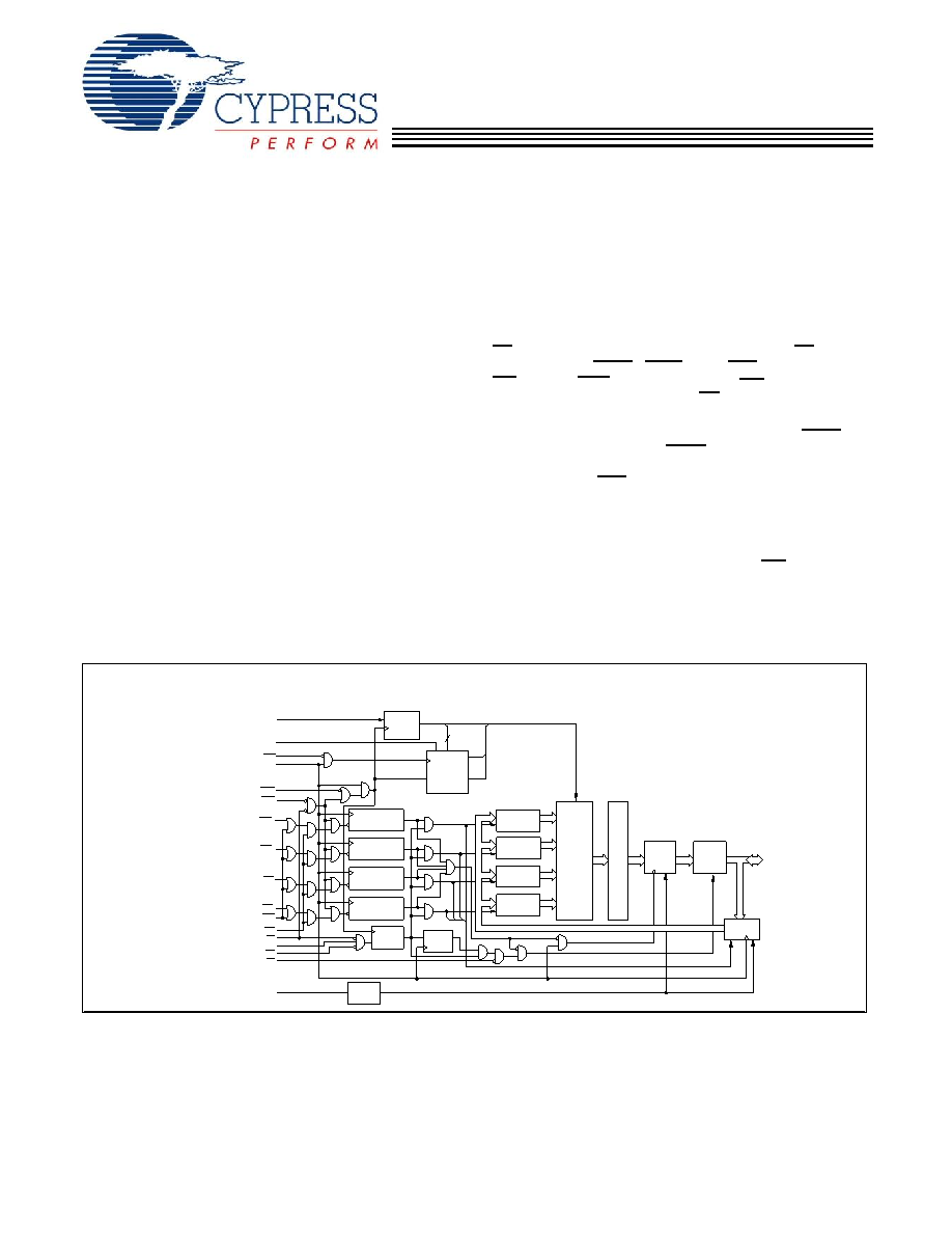
A DDRESS
REGISTER
ADV
CLK
BURST
COUNTER
AND
LOGIC
CLR
Q1
Q0
ADSP
ADSC
MODE
BW E
GW
CE1
CE2
CE3
OE
ENA BLE
REGISTER
OUTPUT
REGISTERS
SENSE
AM PS
OUTPUT
BUFFERS
E
PIPELINED
ENA BLE
INPUT
REGISTERS
A0, A 1, A
BW B
BW C
BW D
BW A
MEMORY
A RRA Y
DQ s
SLEEP
CONTROL
ZZ
A [1:0]
2
DQA
BY TE
W RITE REGISTER
DQB
BY TE
WRITE REGISTER
DQC
BY TE
W RITE REGISTER
DQD
BY TE
WRITE REGISTER
DQA
BY TE
WRITE DRIVER
DQB
BY TE
WRITE DRIVER
DQC
BY TE
WRITE DRIVER
DQD
BY TE
WRITE DRIVER
Logic Block Diagram
相關(guān)PDF資料 |
PDF描述 |
|---|---|
| CY7C1347D-250BGC | 128K X 36 CACHE SRAM, 2.4 ns, PBGA119 |
| CY7C1512JV18-267BZXC | 4M X 18 QDR SRAM, 0.45 ns, PBGA165 |
| CY7C1515AV18-250BZXI | 2M X 36 QDR SRAM, 0.45 ns, PBGA165 |
| CY7C1522JV18-250BZI | 8M X 8 DDR SRAM, 0.45 ns, PBGA165 |
| CY7C1524KV18-333BZI | 2M X 36 DDR SRAM, 0.45 ns, PBGA165 |
相關(guān)代理商/技術(shù)參數(shù) |
參數(shù)描述 |
|---|---|
| CY7C1339G-200BGI | 功能描述:靜態(tài)隨機(jī)存取存儲(chǔ)器 128Kx32 3.3V IND Sync FT 靜態(tài)隨機(jī)存取存儲(chǔ)器 RoHS:否 制造商:Cypress Semiconductor 存儲(chǔ)容量:16 Mbit 組織:1 M x 16 訪問時(shí)間:55 ns 電源電壓-最大:3.6 V 電源電壓-最小:2.2 V 最大工作電流:22 uA 最大工作溫度:+ 85 C 最小工作溫度:- 40 C 安裝風(fēng)格:SMD/SMT 封裝 / 箱體:TSOP-48 封裝:Tray |
| CY7C1339G-200BGIT | 功能描述:靜態(tài)隨機(jī)存取存儲(chǔ)器 128Kx32 3.3V IND Sync FT 靜態(tài)隨機(jī)存取存儲(chǔ)器 RoHS:否 制造商:Cypress Semiconductor 存儲(chǔ)容量:16 Mbit 組織:1 M x 16 訪問時(shí)間:55 ns 電源電壓-最大:3.6 V 電源電壓-最小:2.2 V 最大工作電流:22 uA 最大工作溫度:+ 85 C 最小工作溫度:- 40 C 安裝風(fēng)格:SMD/SMT 封裝 / 箱體:TSOP-48 封裝:Tray |
| CY7C1339G-200BGXI | 制造商:Cypress Semiconductor 功能描述:SRAM SYNC QUAD 3.3V 4MBIT 128KX32 2.8NS 119BGA - Bulk |
| CY7C1339L-15ZIT | 制造商:Cypress Semiconductor 功能描述:ELECTRONIC COMPONENT |
| CY7C1339S-133AXC | 功能描述:靜態(tài)隨機(jī)存取存儲(chǔ)器 CY7C1339S-133AXC RoHS:否 制造商:Cypress Semiconductor 存儲(chǔ)容量:16 Mbit 組織:1 M x 16 訪問時(shí)間:55 ns 電源電壓-最大:3.6 V 電源電壓-最小:2.2 V 最大工作電流:22 uA 最大工作溫度:+ 85 C 最小工作溫度:- 40 C 安裝風(fēng)格:SMD/SMT 封裝 / 箱體:TSOP-48 封裝:Tray |
發(fā)布緊急采購,3分鐘左右您將得到回復(fù)。