- 您現(xiàn)在的位置:買賣IC網(wǎng) > PDF目錄298975 > CY7C1009-15PC (CYPRESS SEMICONDUCTOR CORP) 128K X 8 STANDARD SRAM, 15 ns, PDIP32 PDF資料下載
參數(shù)資料
| 型號: | CY7C1009-15PC |
| 廠商: | CYPRESS SEMICONDUCTOR CORP |
| 元件分類: | SRAM |
| 英文描述: | 128K X 8 STANDARD SRAM, 15 ns, PDIP32 |
| 封裝: | 0.300 INCH, PLASTIC, DIP-32 |
| 文件頁數(shù): | 5/10頁 |
| 文件大?。?/td> | 245K |
| 代理商: | CY7C1009-15PC |
CY7C1009
4
PRELIMINARY
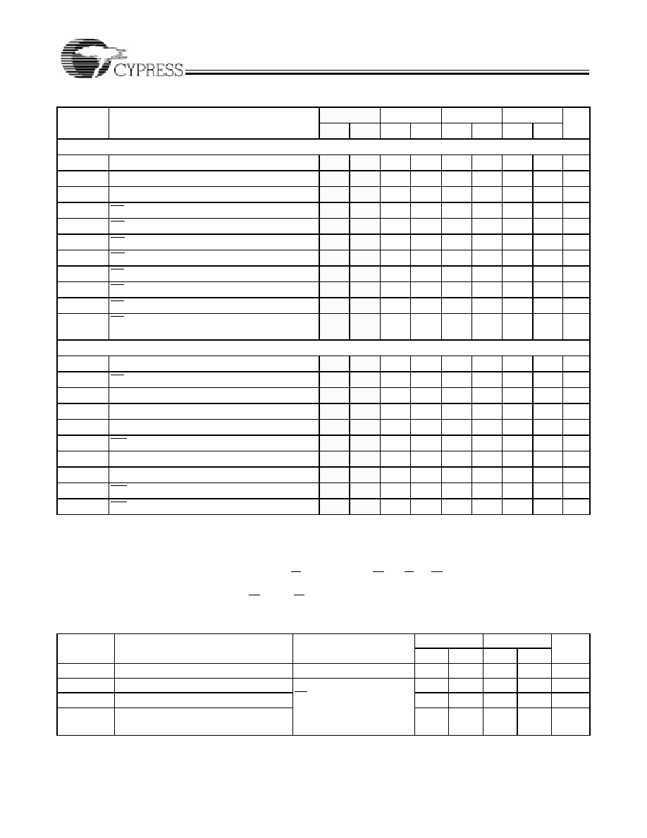
Switching Characteristics Over the Operating Range[3, 6]
7C1009–12
7C1009–15
7C1009–20
7C1009–25
Parameter
Description
Min.
Max.
Min.
Max.
Min.
Max.
Min.
Max.
Unit
READ CYCLE
tRC
Read Cycle Time
12
15
20
25
ns
tAA
Address to Data Valid
12
15
20
25
ns
tOHA
Data Hold from Address Change
3
33
3
ns
tACE
CE1 LOW to Data Valid, CE2 HIGH to Data Valid
12
15
20
25
ns
tDOE
OE LOW to Data Valid
67
8
10
ns
tLZOE
OE LOW to Low Z
0
00
0
ns
tHZOE
OE HIGH to High Z[7, 8]
67
8
10
ns
tLZCE
CE1 LOW to Low Z, CE2 HIGH to Low Z
[8]
3
33
3
ns
tHZCE
CE1 HIGH to High Z, CE2 LOW to High Z
[7, 8]
67
8
10
ns
tPU
CE1 LOW to Power-Up, CE2 HIGH to Power-Up
0
00
0
ns
tPD
CE1 HIGH to Power-Down,
CE2 LOW to Power-Down
12
15
20
25
ns
WRITE CYCLE[9, 10]
tWC
Write Cycle Time
12
15
20
25
ns
tSCE
CE1 LOW to Write End, CE2 HIGH to Write End
10
12
15
20
ns
tAW
Address Set-Up to Write End
10
12
15
20
ns
tHA
Address Hold from Write End
0
00
0
ns
tSA
Address Set-Up to Write Start
0
00
0
ns
tPWE
WE Pulse Width
10
12
15
20
ns
tSD
Data Set-Up to Write End
7
810
15
ns
tHD
Data Hold from Write End
0
00
0
ns
tLZWE
WE HIGH to Low Z[8]
3
33
3
ns
tHZWE
WE LOW to High Z[7, 8]
67
8
10
ns
Shaded area contains advanced information.
Notes:
6.
Test conditions assume signal transition time of 3 ns or less, timing reference levels of 1.5V, input pulse levels of 0 to 3.0V, and output loading of the specified
IOL/IOH and 30-pF load capacitance.
7.
tHZOE, tHZCE, and tHZWE are specified with a load capacitance of 5 pF as in part (b) of AC Test Loads. Transition is measured ±500 mV from steady-state voltage.
8.
At any given temperature and voltage condition, tHZCE is less than tLZCE, tHZOE is less than tLZOE, and tHZWE is less than tLZWE for any given device.
9.
The internal write time of the memory is defined by the overlap of CE1 LOW, CE2 HIGH, and WE LOW. CE1 and WE must be LOW and CE2 HIGH to initiate a write,
and the transition of any of these signals can terminate the write. The input data set-up and hold timing should be referenced to the leading edge of the signal that terminates
the write.
10. The minimum write cycle time for Write Cycle No. 3 (WE controlled, OE LOW) is the sum of tHZWE and tSD.
Data Retention Characteristics Over the Operating Range (L Version Only)
Parameter
Description
Conditions[11]
Commercial
Military
Unit
Min.
Max.
Min.
Max.
VDR
VCC for Data Retention
2.0
V
ICCDR
Data Retention Current
VCC =VDR = 2.0V,
CE1 ≥ VCC – 0.3V or
CE2 ≤ 0.3V,
VIN ≥ VCC – 0.3V or
VIN ≤ 0.3V
50
70
A
tCDR
[5]
Chip Deselect to Data Retention Time
0
ns
tR
[5]
Operation Recovery Time
tRC
ns
Notes:
11.
No input may exceed VCC + 0.5V.
相關(guān)PDF資料 |
PDF描述 |
|---|---|
| CY7C1016-15VCT | 256K X 4 STANDARD SRAM, 15 ns, PDSO32 |
| CY7C1020CV33-10ZXCT | 32K X 16 STANDARD SRAM, 10 ns, PDSO44 |
| CY7C1328F-133AC | 256K X 18 CACHE SRAM, 4 ns, PQFP100 |
| CY7C1339B-133BGIT | 128K X 32 CACHE SRAM, 4 ns, PBGA119 |
| CY7C1339G-200AXCT | 128K X 32 CACHE SRAM, 2.8 ns, PQFP100 |
相關(guān)代理商/技術(shù)參數(shù) |
參數(shù)描述 |
|---|---|
| CY7C100915V | 制造商:Cypress Semiconductor 功能描述: |
| CY7C100915VC | 制造商:Cypress Semiconductor 功能描述: |
| CY7C1009-15VC | 制造商:Cypress Semiconductor 功能描述:Static RAM, 128Kx8, 32 Pin, Plastic, SOJ |
| CY7C100915VIT | 制造商:CYPRESS 功能描述:* |
| CY7C1009-20LMB | 制造商:Cypress Semiconductor 功能描述:SRAM Chip Async Single 5V 1M-Bit 128K x 8 20ns 32-Pin LCC |
發(fā)布緊急采購,3分鐘左右您將得到回復(fù)。