- 您現(xiàn)在的位置:買賣IC網(wǎng) > PDF目錄298975 > CY7C1009-15PC (CYPRESS SEMICONDUCTOR CORP) 128K X 8 STANDARD SRAM, 15 ns, PDIP32 PDF資料下載
參數(shù)資料
| 型號(hào): | CY7C1009-15PC |
| 廠商: | CYPRESS SEMICONDUCTOR CORP |
| 元件分類: | SRAM |
| 英文描述: | 128K X 8 STANDARD SRAM, 15 ns, PDIP32 |
| 封裝: | 0.300 INCH, PLASTIC, DIP-32 |
| 文件頁數(shù): | 3/10頁 |
| 文件大?。?/td> | 245K |
| 代理商: | CY7C1009-15PC |
CY7C1009
2
PRELIMINARY
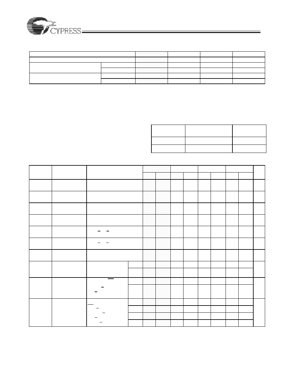
Maximum Ratings
(Above which the useful life may be impaired. For user guide-
lines, not tested.)
Storage Temperature ..................................–65
°C to +150°C
Ambient Temperature with
Power Applied .............................................–55
°C to +125°C
Supply Voltage on VCC to Relative GND
[1].....–0.5V to +7.0V
DC Voltage Applied to Outputs
in High Z State[1] .................................... –0.5V to VCC +0.5V
DC Input Voltage[1] ................................. –0.5V to VCC +0.5V
Current into Outputs (LOW) ......................................... 20 mA
Static Discharge Voltage............................................>2001V
(per MIL-STD-883, Method 3015)
Latch-Up Current .....................................................>200 mA
Selection Guide
7C1009–12
7C1009–15
7C1009–20
7C1009–25
Maximum Access Time (ns)
12
15
20
25
Maximum Operating Current (mA)
Commercial
185
170
155
145
Military
180
170
160
Maximum Standby Current (mA)
Commercial
45
40
30
Military
40
30
Shaded area contains advanced information.
Operating Range
Range
Ambient
Temperature[1]
VCC
Commercial
0
°C to +70°C
5V
± 10%
Military
–55
°C to +125°C
5V
± 10%
Electrical Characteristics Over the Operating Range[3]
7C1009–12
7C1009–15
7C1009–20
7C1009–25
Parameter
Description
Test Conditions
Min.
Max.
Min.
Max.
Min.
Max.
Min.
Max.
Unit
VOH
Output HIGH
Voltage
VCC = Min., IOH = –4.0 mA
2.4
V
VOL
Output LOW
Voltage
VCC = Min., IOL = 8.0 mA
0.4
V
VIH
Input HIGH
Voltage
2.2
VCC
+ 0.3
2.2
VCC
+ 0.3
2.2
VCC
+ 0.3
2.2
VCC
+ 0.3
V
VIL
Input LOW
Voltage[1]
–0.3
0.8
–0.3
0.8
–0.3
0.8
–0.3
0.8
V
IIX
Input Load
Current
GND < VI < VCC
–1
+1
–1
+1
–1
+1
–1
+1
A
IOZ
Output Leakage
Current
GND < VI < VCC,
Output Disabled
–5
+5
–5
+5
–5
+5
–5
+5
A
IOS
Output Short
Circuit Current[4]
VCC = Max., VOUT = GND
–300
mA
ICC
VCC Operating
Supply Current
VCC = Max.,
IOUT = 0 mA,
f = fMAX = 1/tRC
Com’l
185
170
155
145
mA
Mil
180
170
160
ISB1
Automatic CE
Power-Down
Current
—TTL Inputs
Max. VCC, CE1 > VIH
or CE2 < VIL,
VIN > VIH or
VIN < VIL, f = fMAX
Com’l
45
40
30
mA
Mil
40
30
ISB2
Automatic CE
Power-Down
Current
—CMOS Inputs
Max. VCC,
CE1 > VCC – 0.3V,
or CE2 < 0.3V,
VIN > VCC – 0.3V,
or VIN < 0.3V, f=0
Com’l
10
mA
L
2222
Mil
10
L
222
Shaded area contains advanced information.
Notes:
1.
VIL (min.) = –2.0V for pulse durations of less than 20 ns.
2.
TA is the “instant on” case temperature
相關(guān)PDF資料 |
PDF描述 |
|---|---|
| CY7C1016-15VCT | 256K X 4 STANDARD SRAM, 15 ns, PDSO32 |
| CY7C1020CV33-10ZXCT | 32K X 16 STANDARD SRAM, 10 ns, PDSO44 |
| CY7C1328F-133AC | 256K X 18 CACHE SRAM, 4 ns, PQFP100 |
| CY7C1339B-133BGIT | 128K X 32 CACHE SRAM, 4 ns, PBGA119 |
| CY7C1339G-200AXCT | 128K X 32 CACHE SRAM, 2.8 ns, PQFP100 |
相關(guān)代理商/技術(shù)參數(shù) |
參數(shù)描述 |
|---|---|
| CY7C100915V | 制造商:Cypress Semiconductor 功能描述: |
| CY7C100915VC | 制造商:Cypress Semiconductor 功能描述: |
| CY7C1009-15VC | 制造商:Cypress Semiconductor 功能描述:Static RAM, 128Kx8, 32 Pin, Plastic, SOJ |
| CY7C100915VIT | 制造商:CYPRESS 功能描述:* |
| CY7C1009-20LMB | 制造商:Cypress Semiconductor 功能描述:SRAM Chip Async Single 5V 1M-Bit 128K x 8 20ns 32-Pin LCC |
發(fā)布緊急采購,3分鐘左右您將得到回復(fù)。