- 您現(xiàn)在的位置:買賣IC網(wǎng) > PDF目錄11581 > ENC424J600T-I/ML (Microchip Technology)IC ETHERNET CTRLR W/SPI 44-QFN PDF資料下載
參數(shù)資料
| 型號(hào): | ENC424J600T-I/ML |
| 廠商: | Microchip Technology |
| 文件頁數(shù): | 82/168頁 |
| 文件大小: | 0K |
| 描述: | IC ETHERNET CTRLR W/SPI 44-QFN |
| 視頻文件: | Fast 100 Mbps Ethernet PICtail Plus Overview |
| 標(biāo)準(zhǔn)包裝: | 1,600 |
| 控制器類型: | 以太網(wǎng)控制器(IEEE 802.3) |
| 接口: | SPI |
| 電源電壓: | 3 V ~ 3.6 V |
| 電流 - 電源: | 96mA |
| 工作溫度: | -40°C ~ 85°C |
| 安裝類型: | 表面貼裝 |
| 封裝/外殼: | 44-VQFN 裸露焊盤 |
| 供應(yīng)商設(shè)備封裝: | 44-QFN(8x8) |
| 包裝: | 帶卷 (TR) |
| 配用: | AC164132-ND - BOARD DAUGHTER PICTAIL ETHERNET |
第1頁第2頁第3頁第4頁第5頁第6頁第7頁第8頁第9頁第10頁第11頁第12頁第13頁第14頁第15頁第16頁第17頁第18頁第19頁第20頁第21頁第22頁第23頁第24頁第25頁第26頁第27頁第28頁第29頁第30頁第31頁第32頁第33頁第34頁第35頁第36頁第37頁第38頁第39頁第40頁第41頁第42頁第43頁第44頁第45頁第46頁第47頁第48頁第49頁第50頁第51頁第52頁第53頁第54頁第55頁第56頁第57頁第58頁第59頁第60頁第61頁第62頁第63頁第64頁第65頁第66頁第67頁第68頁第69頁第70頁第71頁第72頁第73頁第74頁第75頁第76頁第77頁第78頁第79頁第80頁第81頁當(dāng)前第82頁第83頁第84頁第85頁第86頁第87頁第88頁第89頁第90頁第91頁第92頁第93頁第94頁第95頁第96頁第97頁第98頁第99頁第100頁第101頁第102頁第103頁第104頁第105頁第106頁第107頁第108頁第109頁第110頁第111頁第112頁第113頁第114頁第115頁第116頁第117頁第118頁第119頁第120頁第121頁第122頁第123頁第124頁第125頁第126頁第127頁第128頁第129頁第130頁第131頁第132頁第133頁第134頁第135頁第136頁第137頁第138頁第139頁第140頁第141頁第142頁第143頁第144頁第145頁第146頁第147頁第148頁第149頁第150頁第151頁第152頁第153頁第154頁第155頁第156頁第157頁第158頁第159頁第160頁第161頁第162頁第163頁第164頁第165頁第166頁第167頁第168頁
PIC16CR7X
DS21993C-page 18
2007 Microchip Technology Inc.
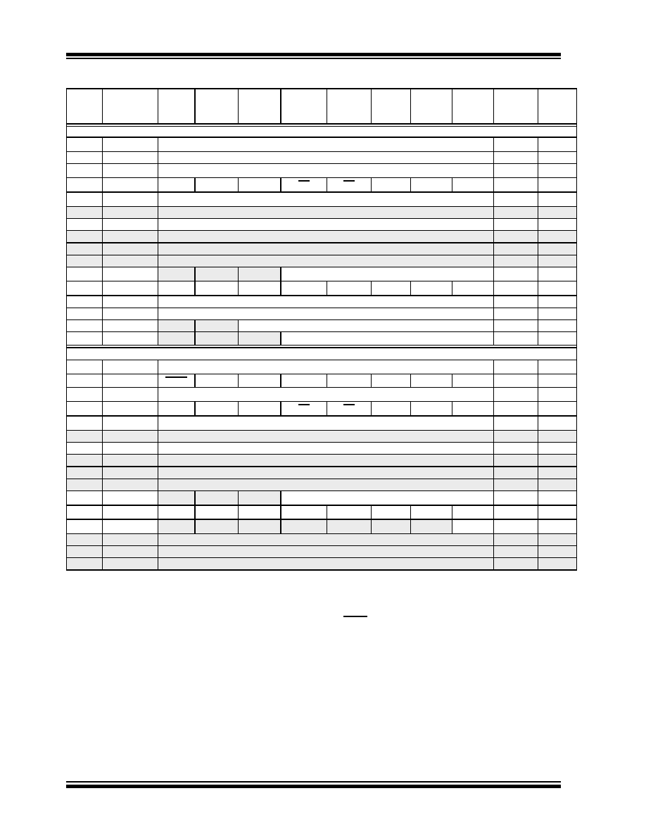
Bank 2
100h(4)
INDF
Addressing this location uses contents of FSR to address data memory (not a physical register)
0000 0000
101h
TMR0
Timer0 Module Register
xxxx xxxx
102h(4)
PCL
Program Counter (PC) Least Significant Byte
0000 0000
103h(4)
STATUS
IRP
RP1
RP0
TO
PD
ZDC
C
0001 1xxx
104h(4)
FSR
Indirect Data Memory Address Pointer
xxxx xxxx
105h
—
Unimplemented
—
106h
PORTB
PORTB Data Latch when written: PORTB pins when read
xxxx xxxx
107h
—
Unimplemented
—
108h
—
Unimplemented
—
109h
—
Unimplemented
—
10Ah(1,4) PCLATH
—
Write Buffer for the upper 5 bits of the Program Counter
---0 0000
10Bh(4)
INTCON
GIE
PEIE
TMR0IE
INTE
RBIE
TMR0IF
INTF
RBIF
0000 000x
10Ch
PMDATA
Data Register Low Byte
xxxx xxxx
10Dh
PMADR
Address Register Low Byte
xxxx xxxx
10Eh
PMDATH
—
Data Register High Byte
xxxx xxxx
10Fh
PMADRH
—
Address Register High Byte
xxxx xxxx
Bank 3
180h(4)
INDF
Addressing this location uses contents of FSR to address data memory (not a physical register)
0000 0000
181h
OPTION_REG
RBPU
INTEDG
T0CS
T0SE
PSA
PS2
PS1
PS0
1111 1111
182h(4)
PCL
Program Counter (PC) Least Significant Byte
0000 0000
183h(4)
STATUS
IRP
RP1
RP0
TO
PD
ZDC
C
0001 1xxx
184h(4)
FSR
Indirect Data Memory Address Pointer
xxxx xxxx
185h
—
Unimplemented
—
186h
TRISB
PORTB Data Direction Register
1111 1111
187h
—
Unimplemented
—
188h
—
Unimplemented
—
189h
—
Unimplemented
—
18Ah(1,4) PCLATH
—
Write Buffer for the upper 5 bits of the Program Counter
---0 0000
18Bh(4)
INTCON
GIE
PEIE
TMR0IE
INTE
RBIE
TMR0IF
INTF
RBIF
0000 000x
18Ch
PMCON1
— (6)
—
—RD
1--- ---0
18Dh
—
Unimplemented
—
18Eh
—
Reserved maintain clear
0000 0000
18Fh
—
Reserved maintain clear
0000 0000
TABLE 2-1:
SPECIAL FUNCTION REGISTER SUMMARY (CONTINUED)
Address
Name
Bit 7
Bit 6
Bit 5
Bit 4
Bit 3
Bit 2
Bit 1
Bit 0
Value on
POR,
BOR
Details
on page
Legend:
x
= unknown, u = unchanged, q = value depends on condition, – = unimplemented, read as ‘0’, r = reserved.
Shaded locations are unimplemented, read as ‘0’.
Note
1:
The upper byte of the program counter is not directly accessible. PCLATH is a holding register for the PC<12:8>, whose
contents are transferred to the upper byte of the program counter during branches (CALL or GOTO).
2:
Other (non Power-up) Resets include external Reset through MCLR and Watchdog Timer Reset.
3:
Bits PSPIE and PSPIF are reserved on the 28-pin devices; always maintain these bits clear.
4:
These registers can be addressed from any bank.
5:
PORTD, PORTE, TRISD and TRISE are not physically implemented on the 28-pin devices, read as ‘0’.
6:
This bit always reads as a ‘1’.
相關(guān)PDF資料 |
PDF描述 |
|---|---|
| PIC16F677-E/P | IC PIC MCU FLASH 2KX14 20DIP |
| MCP2155-I/P | IC IRDA PROTOCOL CTRLR 18DIP |
| MCP2150T-I/SS | IC IRDA STD CONTROLLER 20SSOP |
| MCP2155T-I/SO | IC IRDA PROTOCOL CONTRLR 18-SOIC |
| PIC18F25J10T-I/SS | IC PIC MCU FLASH 16KX16 28SSOP |
相關(guān)代理商/技術(shù)參數(shù) |
參數(shù)描述 |
|---|---|
| ENC424J600T-IPT | 制造商:MICROCHIP 制造商全稱:Microchip Technology 功能描述:Stand-Alone 10/100 Ethernet Controller with SPI or Parallel Interface |
| ENC431D05A | 制造商:未知廠家 制造商全稱:未知廠家 功能描述: |
| ENC431D-05A | 制造商:未知廠家 制造商全稱:未知廠家 功能描述:STD MOV |
| ENC431D07A | 制造商:未知廠家 制造商全稱:未知廠家 功能描述: |
| ENC431D-07A | 制造商:未知廠家 制造商全稱:未知廠家 功能描述:STD MOV |
發(fā)布緊急采購,3分鐘左右您將得到回復(fù)。