- 您現(xiàn)在的位置:買賣IC網(wǎng) > PDF目錄382968 > FS6232-01 (Electronic Theatre Controls, Inc.) TWO WAY MP MOTHERBOARD CLOCK GENERATOR IC PDF資料下載
參數(shù)資料
| 型號: | FS6232-01 |
| 廠商: | Electronic Theatre Controls, Inc. |
| 英文描述: | TWO WAY MP MOTHERBOARD CLOCK GENERATOR IC |
| 中文描述: | 雙向手機主板時鐘發(fā)生器芯片 |
| 文件頁數(shù): | 5/14頁 |
| 文件大?。?/td> | 194K |
| 代理商: | FS6232-01 |
AMERICAN MICROSYSTEMS, INC.
September 2000
9.18.00
5
FS6232-01
Two-Way MP Motherboard Clock Generator IC
ISO9001
4.0 Power Management
The PWR_DWN# signal is an asynchronous, active-low
LVTTL input that places the device in a low power inac-
tive state without removing power from the device. All
internal clocks are turned off, and all clock outputs are
held low.
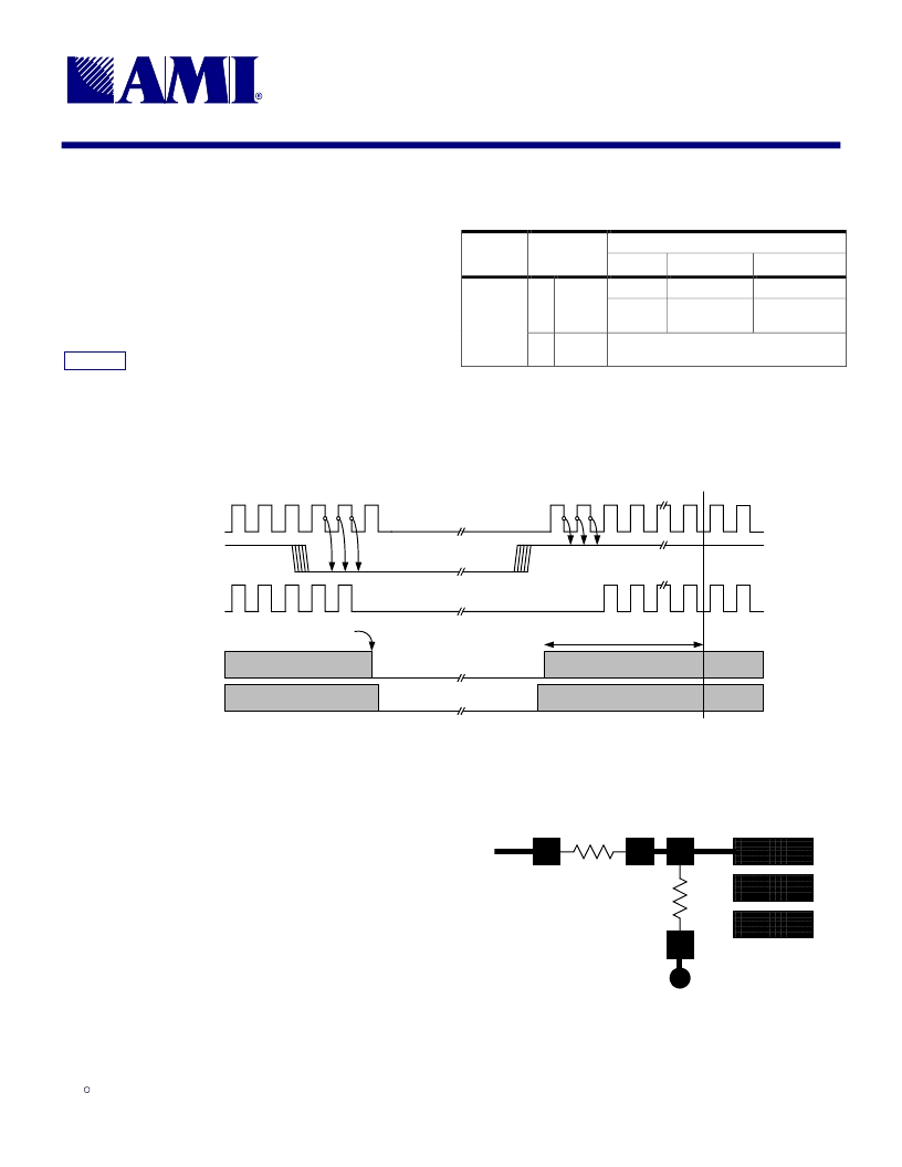
Since PWR_DWN# is asynchronous, the signal is syn-
chronized internally to each individual clock. As shown in
Figure 3, a falling-rising-falling edge sequence on any
individual clock output is required before that clock output
is disabled low. This edge sequence ensures that one
complete clock cycle will occur before the clock stops.
Table 9: Latency Table
LATENCY
SIGNAL
SIGNAL
STATE
MIN.
MAX.
Output:
2 clocks
2
×
REF
clocks
3 clocks
0
Power
OFF
Device:
3
×
REF clocks
PWR_
DWN#
1
Power
ON
3ms
Upon the release of PWR_DWN# (power-up), external
circuitry should allow a minimum of 3ms for the PLL to
lock before enabling any clocks.
Figure 3: PWR_DWN# Timing
Any Clock
(output)
PWR_DWN#
Any Clock
(internal)
VCO
Crystal
Oscillator
After REF
output shuts off...
3ms until clock is valid
Shaded regions in the Crystal Oscillator and VCO waveforms indicate that the clock is valid and the Crystal Oscillator and VCO are active.
5.0 Dual Function I/O Pins
Several pins on this device serve as dual function in-
put/output pins. During the initial application of VDD to
the device, this type of pin functions as an input pin.
Upon completion of power-up, the logic state present on
the pin is latched internally, and the pin is converted to an
output driver.
An external 10k
pull-down resistor to ground is required
for a logic low and a 10k
pull-up resistor to the clock
output VDD is required for a logic high. The 10k
resistor
presents an insignificant load to the output driver that
should not affect the output clock.
Note that the latching of the logic state occurs only on the
application of the chip supply voltage (VDD). The logic
state on the pin is not latched if the PWR_DWN# signal is
used to power-down the device with VDD still applied.
Figure 4: I/O Pin Programming
Clock Trace
Termination
Resistor
Device Solder
Pads
Ground or
Power Via
10k
Programming
Resistor
相關PDF資料 |
PDF描述 |
|---|---|
| FS6261-01 | Motherboard Clock Generator IC |
| FS6284 | Dual PLL Clock Generator IC |
| FS6284-01 | Dual PLL Clock Generator IC |
| FS6322-05 | Three-PLL Clock Generator IC |
| FS6322-08 | THREE PLL CLOCK GENERATOR IC |
相關代理商/技術參數(shù) |
參數(shù)描述 |
|---|---|
| FS6261-01 | 制造商:未知廠家 制造商全稱:未知廠家 功能描述:Motherboard Clock Generator IC |
| FS6282 | 制造商:未知廠家 制造商全稱:未知廠家 功能描述:DUAL PLL CLOCK GENERATOR IC |
| FS6282-03 | 制造商:未知廠家 制造商全稱:未知廠家 功能描述:DUAL PLL CLOCK GENERATOR IC |
| FS6284 | 制造商:未知廠家 制造商全稱:未知廠家 功能描述:Dual PLL Clock Generator IC |
| FS6284-01 | 制造商:未知廠家 制造商全稱:未知廠家 功能描述:Dual PLL Clock Generator IC |
發(fā)布緊急采購,3分鐘左右您將得到回復。