- 您現(xiàn)在的位置:買賣IC網(wǎng) > PDF目錄224008 > ICSSSTUAF32868BHLFT (INTEGRATED DEVICE TECHNOLOGY INC) 32868 SERIES, POSITIVE EDGE TRIGGERED D FLIP-FLOP, TRUE OUTPUT, PBGA176 PDF資料下載
參數(shù)資料
| 型號: | ICSSSTUAF32868BHLFT |
| 廠商: | INTEGRATED DEVICE TECHNOLOGY INC |
| 元件分類: | 鎖存器 |
| 英文描述: | 32868 SERIES, POSITIVE EDGE TRIGGERED D FLIP-FLOP, TRUE OUTPUT, PBGA176 |
| 封裝: | LEAD FREE, MO-205/MO-255/MO-246, LFBGA-176 |
| 文件頁數(shù): | 3/22頁 |
| 文件大小: | 538K |
| 代理商: | ICSSSTUAF32868BHLFT |
ICSSSTUAF32868B
28-BIT CONFIGURABLE REGISTERED BUFFER FOR DDR2
COMMERCIAL TEMPERATURE GRADE
28-BIT CONFIGURABLE REGISTERED BUFFER FOR DDR2
11
ICSSSTUAF32868B
7102/2
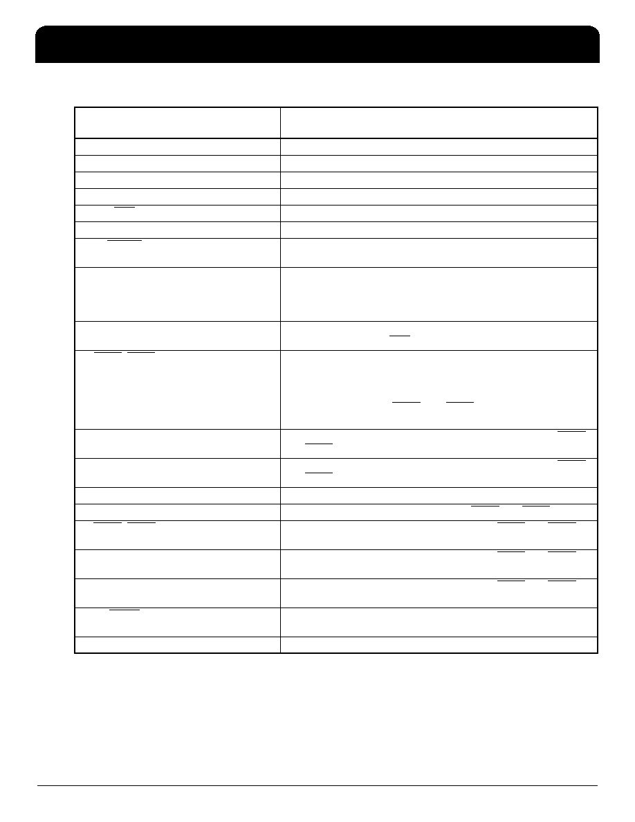
Terminal Functions
Terminal Name
Electrical
Characteristics
Description
GND
Ground Input
Ground
VDD
1.8V nominal
Power Supply Voltage
VREF
0.9V nominal
Input Reference Clock
CLK
Differential Input
Positive Master Clock Input
CLK
Differential Input
Negative Master Clock Input
C
LVCMOS Input
Configuration Control Inputs - Register A or Register B
RESET
LVCMOS Input
Asynchronous Reset Input. Resets registers and disables Vref data
and clock differential-input receivers.
CSGEN
LVCMOS Input
Chip select gate enable – When high, D1-D28 inputs will be latched
only when at least one chip select input is low during the rising edge
of the clock. When low, the D1-D28 inputs will be latched and
redriven on every rising edge of the clock.
D1 - D28
SSTL_18 Input
Data Input. Clocked in on the crossing of the rising edge of CLK
and the falling edge of CLK.
DCS0, DCS1
SSTL_18 Input
Chip select inputs – These pins initiate DRAM address/command
decodes, and as such at least one will be low when a valid
address/command is present. The Register can be programmed to
redrive all D inputs (CSGEN high) only when at least one chip select
input is low. If CSGEN, DCS0, and DCS1 inputs are high, D1-D28
inputs will be disabled.
DCKE0, DCKE1
SSTL_18 Input
The outputs of this register bit will not be suspended by the DCS0
and DCS1 controls
DODT0, DODT1
SSTL_18 Input
The outputs of this register bit will not be suspended by the DCS0
and DCS1 controls
PAR_IN
SSTL_18 Input
Parity Input arrives one cycle after corresponding data input
Q1 - Q28
1.8V CMOS
Data Outputs that are suspended by the DCS0 and DCS1 controls
QCS0, QCS1
1.8V CMOS
Data Output that will not be suspended by the DCS0 and DCS1
controls
QCKE0, QCKE1
1.8V CMOS
Data Output that will not be suspended by the DCS0 and DCS1
controls
QODT0, QODT1
1.8V CMOS
Data Output that will not be suspended by the DCS0 and DCS1
controls
QERR
Open Drain Output
Output Error bit, generated one cycle after the corresponding data
output
NC
No Connection
相關(guān)PDF資料 |
PDF描述 |
|---|---|
| IDT2309-1HDCGI8 | PLL BASED CLOCK DRIVER, 8 TRUE OUTPUT(S), 0 INVERTED OUTPUT(S), PDSO16 |
| IDT54FCT373CTEB | FCT SERIES, 8-BIT DRIVER, TRUE OUTPUT, CDFP20 |
| IDT5V996BBI | 5V SERIES, PLL BASED CLOCK DRIVER, 8 TRUE OUTPUT(S), 0 INVERTED OUTPUT(S), PBGA144 |
| IDT5V996BBI8 | 5V SERIES, PLL BASED CLOCK DRIVER, 8 TRUE OUTPUT(S), 0 INVERTED OUTPUT(S), PBGA144 |
| IDT71258L35TP | 64K X 4 STANDARD SRAM, 35 ns, PDIP24 |
相關(guān)代理商/技術(shù)參數(shù) |
參數(shù)描述 |
|---|---|
| ICSSSTUAF32869A | 制造商:IDT 制造商全稱:Integrated Device Technology 功能描述:14-BIT CONFIGURABLE REGISTERED BUFFER FOR DDR2 |
| ICSSSTUAF32869AHLF | 制造商:IDT 制造商全稱:Integrated Device Technology 功能描述:14-BIT CONFIGURABLE REGISTERED BUFFER FOR DDR2 |
| ICSSSTUAH32865A | 制造商:IDT 制造商全稱:Integrated Device Technology 功能描述:25-BIT CONFIGURABLE REGISTERED BUFFER FOR DDR2 |
| ICSSSTUAH32865AHLFT | 制造商:IDT 制造商全稱:Integrated Device Technology 功能描述:25-BIT CONFIGURABLE REGISTERED BUFFER FOR DDR2 |
| ICSSSTUAH32868A | 制造商:IDT 制造商全稱:Integrated Device Technology 功能描述:28-BIT CONFIGURABLE REGISTERED BUFFER FOR DDR2 |
發(fā)布緊急采購,3分鐘左右您將得到回復(fù)。