- 您現(xiàn)在的位置:買賣IC網(wǎng) > PDF目錄67716 > IDT82V3155PVG8 (INTEGRATED DEVICE TECHNOLOGY INC) PLL BASED CLOCK DRIVER, 7 TRUE OUTPUT(S), 5 INVERTED OUTPUT(S), PDSO56 PDF資料下載
參數(shù)資料
| 型號: | IDT82V3155PVG8 |
| 廠商: | INTEGRATED DEVICE TECHNOLOGY INC |
| 元件分類: | 時(shí)鐘及定時(shí) |
| 英文描述: | PLL BASED CLOCK DRIVER, 7 TRUE OUTPUT(S), 5 INVERTED OUTPUT(S), PDSO56 |
| 封裝: | SSOP-56 |
| 文件頁數(shù): | 28/30頁 |
| 文件大?。?/td> | 406K |
| 代理商: | IDT82V3155PVG8 |
第1頁第2頁第3頁第4頁第5頁第6頁第7頁第8頁第9頁第10頁第11頁第12頁第13頁第14頁第15頁第16頁第17頁第18頁第19頁第20頁第21頁第22頁第23頁第24頁第25頁第26頁第27頁當(dāng)前第28頁第29頁第30頁
7
IDT82V3155 ENHANCED T1/E1/OC3 WAN PLL WITH DUAL REFERENCE INPUTS
INDUSTRIAL TEMPERATURE
1
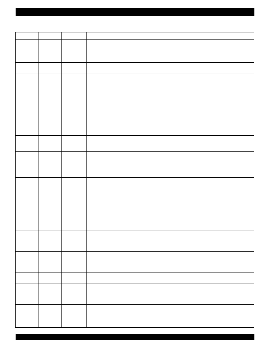
PIN DESCRIPTION
Name
Type
Pin Number
Description
VSS
Power
12, 18, 27
38, 47
Ground.
0 V. All VSS pins should be connected to the ground.
VDD
Power
13, 19, 26
37, 48
Positive Supply Voltage.
All VDD pins should be connected to +3.3 V (nominal).
OSCi
(CMOS) I
50
Oscillator Master Clock Input.
This pin is connected to a clock source.
Fref0
Fref1
I
5
6
Reference Input 0 and Reference Input 1.
These are two input reference sources (falling edge of 8 kHz, 1.544 MHz and 2.048 MHz or rising edge of 19.44
MHz) used for synchronization. The IN_sel pin determines which one of the two reference inputs to be used. See
Table - 4 for details.
The frequency of the reference inputs can be 8 kHz, 1.544 MHz, 2.048 MHz or 19.44 MHz. These two pins are
internally pulled up to VDD.
IN_sel
I11
Input Reference Selection.
A logic low at this pin selects Reference Input 0 (Fref0) and a logic high at this pin selects Reference Input 1 (Fref1).
The logic level on this input is gated in by the rising edges of F8o. This Pin is internally pulled down to VSS.
F0_sel0
F0_sel1
I
9
10
Frequency Selection Inputs for Fref0.
These two inputs select one of the four possible frequencies (8 kHz, 1.544 MHz, 2.048 MHz or 19.44 MHz) for the
Reference Input 0 (Fref0). See Table - 2 for details.
F1_sel0
F1_sel1
I
35
34
Frequency Selection Inputs for Fref1.
These two inputs select one of the four possible frequencies (8 kHz, 1.544 MHz, 2.048 MHz or 19.44 MHz) for the
Reference Input 1 (Fref1). These two pins are internally pulled down to Vss. See Table - 3 for details.
MODE_sel0
MODE_sel1
I
1
2
Mode Selection Inputs.
These two inputs determine the operating mode of the IDT82V3155 (Normal, Holdover or Freerun). See Table - 1
for details.
The logic levels on these two pins are gated in by the rising edges of F8o. These two pins are internally pulled down
to VSS.
RST
I4
Reset Input.
Pulling this pin to logic low for at least 300 ns will reset the IDT82V3155. While the RST pin is low, all framing and
clock outputs are at logic high.
To ensure proper operation, the device must be reset after it is powered up.
TCLR
I3
TIE Control Block Reset.
Pulling this pin to logic low for at least 300 ns will reset the TIE (Maximum Time Interval Error) control block and
result in a realignment of the output phase with the input phase. This pin is internally pulled up to VDD.
TIE_en
I56
TIE Control Block Enable.
A logic high at this pin enables the TIE control block while a logic low disables it. The logic level on this input is gated
in by the rising edges of F8o. This pin is internally pulled down to Vss.
FLOCK
I45
Fast Lock Mode Enable.
When this pin is set to logic high, the DPLL will quickly lock to the input reference within 500 ms.
LOCK
(CMOS) O
44
Lock Indicator.
This output pin will go high when the DPLL is frequency locked to the input reference.
HOLDOVER
(CMOS) O
52
Holdover Indicator.
This output pin will go high whenever the DPLL enters Holdover mode.
NORMAL
(CMOS) O
46
Normal Indicator.
This output pin will go high whenever the DPLL enters Normal mode.
FREERUN
(CMOS) O
51
Freerun Indicator.
This output pin will go high whenever the DPLL enters Freerun mode.
MON_out0
O
7
Frequency Out-of-range Indicator for Fref0.
A logic high at this pin indicates that Fref0 is off the nominal frequency by more than ±12 ppm.
MON_out1
O
8
Frequency Out-of-range Indicator for Fref1.
A logic high at this pin indicates that Fref1 is off the nominal frequency by more than ±12 ppm.
C155POS
C155NEG
(LVDS) O
21
22
155.52 MHz Clock Output (LVDS Level).
This pair of pins output a 155.52 MHz clock, used for OC3/STS3 and SDH/SONET applications.
C19o
(CMOS) O
43
19.44 MHz Clock Output (CMOS Level).
This output is a 19.44 MHz clock used for OC3/STS3 applications.
相關(guān)PDF資料 |
PDF描述 |
|---|---|
| IDT85304-01PGGI8 | 85304 SERIES, LOW SKEW CLOCK DRIVER, 5 TRUE OUTPUT(S), 0 INVERTED OUTPUT(S), PDSO20 |
| IDT8535-01PGG8 | 8535 SERIES, LOW SKEW CLOCK DRIVER, 4 TRUE OUTPUT(S), 4 INVERTED OUTPUT(S), PDSO20 |
| IDT8737-11PGG8 | 8737 SERIES, LOW SKEW CLOCK DRIVER, 4 TRUE OUTPUT(S), 0 INVERTED OUTPUT(S), PDSO20 |
| IDT8737-11PGI8 | 8737 SERIES, LOW SKEW CLOCK DRIVER, 4 TRUE OUTPUT(S), 0 INVERTED OUTPUT(S), PDSO20 |
| IDTCSPT857BV8 | CSPT857 SERIES, PLL BASED CLOCK DRIVER, 10 TRUE OUTPUT(S), 0 INVERTED OUTPUT(S), BGA56 |
相關(guān)代理商/技術(shù)參數(shù) |
參數(shù)描述 |
|---|---|
| IDT82V3202 | 制造商:IDT 制造商全稱:Integrated Device Technology 功能描述:EBU WAN PLL |
| IDT82V32021 | 制造商:IDT 制造商全稱:Integrated Device Technology 功能描述:EBU WAN PLL |
| IDT82V32021NLBLANK | 制造商:IDT 制造商全稱:Integrated Device Technology 功能描述:EBU WAN PLL |
| IDT82V32021NLGBLANK | 制造商:IDT 制造商全稱:Integrated Device Technology 功能描述:EBU WAN PLL |
| IDT82V3202EDGBLANK | 制造商:IDT 制造商全稱:Integrated Device Technology 功能描述:EBU WAN PLL |
發(fā)布緊急采購,3分鐘左右您將得到回復(fù)。