- 您現(xiàn)在的位置:買賣IC網(wǎng) > PDF目錄373088 > K9K1G08U0A1 (SAMSUNG SEMICONDUCTOR CO. LTD.) 128M x 8 Bit / 64M x 16 Bit NAND Flash Memory PDF資料下載
參數(shù)資料
| 型號: | K9K1G08U0A1 |
| 廠商: | SAMSUNG SEMICONDUCTOR CO. LTD. |
| 英文描述: | 128M x 8 Bit / 64M x 16 Bit NAND Flash Memory |
| 中文描述: | 128M的× 8位/ 64米× 16位NAND閃存 |
| 文件頁數(shù): | 15/43頁 |
| 文件大?。?/td> | 906K |
| 代理商: | K9K1G08U0A1 |
第1頁第2頁第3頁第4頁第5頁第6頁第7頁第8頁第9頁第10頁第11頁第12頁第13頁第14頁當(dāng)前第15頁第16頁第17頁第18頁第19頁第20頁第21頁第22頁第23頁第24頁第25頁第26頁第27頁第28頁第29頁第30頁第31頁第32頁第33頁第34頁第35頁第36頁第37頁第38頁第39頁第40頁第41頁第42頁第43頁
FLASH MEMORY
15
K9K1G08U0A
K9K1G08Q0A
K9K1G16U0A
K9K1G16Q0A
Preliminary
*
Check "FFh" at the column address 512
of the 1st and 2nd page in the block
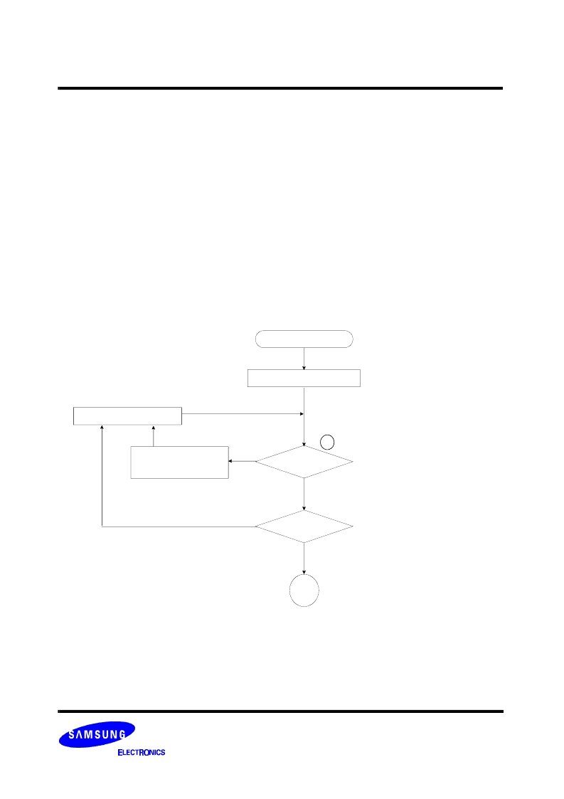
Figure 4. Flow chart to create invalid block table.
Start
Set Block Address = 0
Check "FFh"
Increment Block Address
Last Block
End
No
Yes
Yes
Create (or update)
Invalid Block(s) Table
No
NAND Flash Technical Notes
Invalid Block(s)
Invalid blocks are defined as blocks that contain one or more invalid bits whose reliability is not guaranteed by Samsung. The infor-
mation regarding the invalid block(s) is so called as the invalid block information. Devices with invalid block(s) have the same quality
level as devices with all valid blocks and have the same AC and DC characteristics. An invalid block(s) does not affect the perfor-
mance of valid block(s) because it is isolated from the bit line and the common source line by a select transistor. The system design
must be able to mask out the invalid block(s) via address mapping. The 1st block, which is placed on 00h block address, is fully guar-
anteed to be a valid block, does not require Error Correction.
Identifying Invalid Block(s)
All device locations are erased(FFh) except locations where the invalid block(s) information is written prior to shipping. The invalid
block(s) status is defined by the 6th byte(X8 device) or 1st word(X16 device) in the spare area. Samsung makes sure that either the
1st or 2nd page of every invalid block has non-FFh(X8 device) or non-FFFFh(X16 device) data at the column address of 517(X8
device) or 256 and 261(X16 device). Since the invalid block information is also erasable in most cases, it is impossible to recover the
information once it has been erased. Therefore, the system must be able to recognize the invalid block(s) based on the original
invalid block information and create the invalid block table via the following suggested flow chart(Figure 4). Any intentional erasure of
the original invalid block information is prohibited.
相關(guān)PDF資料 |
PDF描述 |
|---|---|
| K9K1G16Q0A | 128M x 8 Bit / 64M x 16 Bit NAND Flash Memory |
| K9K1G16U0A | 128M x 8 Bit / 64M x 16 Bit NAND Flash Memory |
| K9K2G08U1A | 128M x 8 Bit / 256M x 8 Bit NAND Flash Memory |
| K9F1G08R0A | Circular Connector; MIL SPEC:MIL-DTL-38999 Series III; Body Material:Metal; Series:TVP00; No. of Contacts:99; Connector Shell Size:25; Connecting Termination:Crimp; Circular Shell Style:Wall Mount Receptacle; Body Style:Straight |
| K9K2G16Q0M-YIB0 | 256M x 8 Bit / 128M x 16 Bit NAND Flash Memory |
相關(guān)代理商/技術(shù)參數(shù) |
參數(shù)描述 |
|---|---|
| K9K1G08U0B | 制造商:SAMSUNG 制造商全稱:Samsung semiconductor 功能描述:128M x 8 Bit NAND Flash Memory |
| K9K1G08U0B-JIB0000 | 制造商:Samsung Semiconductor 功能描述:1GB SLC DIE STACK X8 FBGA - Trays |
| K9K1G08U0M | 制造商:SAMSUNG 制造商全稱:Samsung semiconductor 功能描述:nand flash |
| K9K1G08U0M-YCB0 | 制造商:SAMSUNG 制造商全稱:Samsung semiconductor 功能描述:nand flash |
| K9K1G08U0M-YIB0 | 制造商:SAMSUNG 制造商全稱:Samsung semiconductor 功能描述:nand flash |
發(fā)布緊急采購,3分鐘左右您將得到回復(fù)。