- 您現(xiàn)在的位置:買(mǎi)賣IC網(wǎng) > PDF目錄370837 > M32000D4 (Mitsubishi Electric Corporation) SINGLE CHIP 32 BIT CMOS MICROCOMPUTER PDF資料下載
參數(shù)資料
| 型號(hào): | M32000D4 |
| 廠商: | Mitsubishi Electric Corporation |
| 英文描述: | SINGLE CHIP 32 BIT CMOS MICROCOMPUTER |
| 中文描述: | 單芯片32位CMOS微機(jī) |
| 文件頁(yè)數(shù): | 17/45頁(yè) |
| 文件大?。?/td> | 535K |
| 代理商: | M32000D4 |
第1頁(yè)第2頁(yè)第3頁(yè)第4頁(yè)第5頁(yè)第6頁(yè)第7頁(yè)第8頁(yè)第9頁(yè)第10頁(yè)第11頁(yè)第12頁(yè)第13頁(yè)第14頁(yè)第15頁(yè)第16頁(yè)當(dāng)前第17頁(yè)第18頁(yè)第19頁(yè)第20頁(yè)第21頁(yè)第22頁(yè)第23頁(yè)第24頁(yè)第25頁(yè)第26頁(yè)第27頁(yè)第28頁(yè)第29頁(yè)第30頁(yè)第31頁(yè)第32頁(yè)第33頁(yè)第34頁(yè)第35頁(yè)第36頁(yè)第37頁(yè)第38頁(yè)第39頁(yè)第40頁(yè)第41頁(yè)第42頁(yè)第43頁(yè)第44頁(yè)第45頁(yè)

SINGLE-CHIP 32-BIT CMOS MICROCOMPUTER
MITSUBISHI MICROCOMPUTERS
M32000D4AFP
17
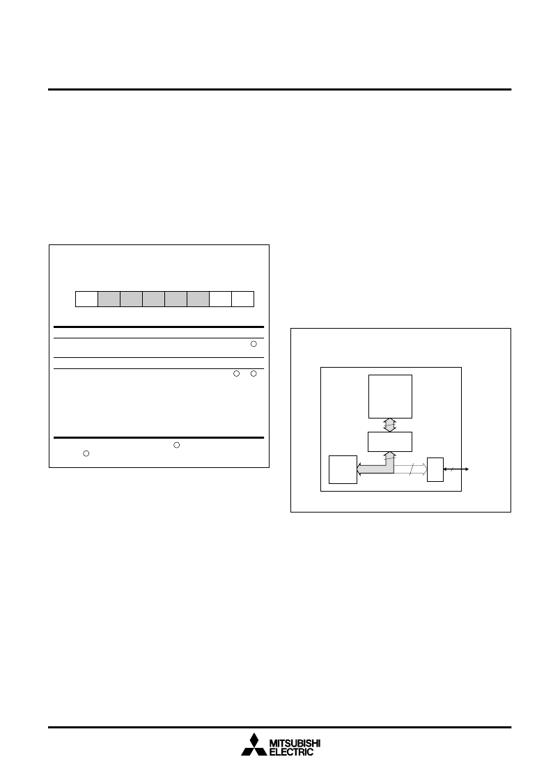
Internal memory system
The memory system built into the M32000D4AFP has the following
characteristics.
internal 16M-bit (2M-byte) DRAM
internal 4K-byte cache memory
CPU, cache and internal DRAM are connected by a 128-bit bus
selectable cache memory operation mode
– internal instruction/data cache mode
– instruction cache mode
– cache-off mode
When the internal instruction/data cache mode is selected, the cache
memory functions as a cache for both instruction and data from the
internal DRAM, and caches all bus access to the DRAM. This mode
is for a system which uses the internal DRAM as main memory. Trans-
fer between the M32R CPU, cache memory and internal DRAM is
always carried out in blocks of 128 bits. Caching is carried out by the
direct map method. Writing is by the copy back method.
When the M32000D4AFP access destination is an external space,
data transfer between the M32R CPU and the external device is car-
ried out via the bus interface unit (BIU). The BIU has a 128-bit data
buffer which converts the bus width between the 128-bit bus in the
M32000D4AFP and the external bus. Caching is not applicable in
this case of data transfer.
When accessing the internal DRAM from an external bus master,
and a cache hit occurs (the accessed data is inside the cache), data
transfer between the cache memory and the external bus via the BIU
is carried out. When a cache miss occurs, (the accessed data is not
inside the cache) data transfer is carried out between the internal
DRAM and the external bus via the BIU without cache replacement.
cache control register (MCCR) < address: H'FFFF FFFF>
D24
D25
D26
D27
D28
D29
D30
D31
CP
CM0
CM1
<at reset: H'01>
R
0
D
24
bit name
CP
(cache purge)
Not assigned.
CM0, CM1
(cache mode)
function
0: no purge
1: purge
W
25 - 29
30, 31
0
00: cache mode
is not changed
01: cache-off mode
10: internal
instruction/data
cache mode
11: instruction cache
mode
R =
... read enabled
W =
: write disabled
R = 0 ... "0" when reading
W =
... write enabled
Fig. 12 Cache control register
Fig. 13 Internal instruction/data cache mode
128
external bus
(16 bits)
16
external bus
interface
M32000D4AFP
128
128
instruction/
data cache
DRAM
BIU
CPU
相關(guān)PDF資料 |
PDF描述 |
|---|---|
| M32000D4AFP | SINGLE CHIP 32 BIT CMOS MICROCOMPUTER |
| M32170F3VFP | SINGLE-CHIP 32-BIT CMOS MICROCOMPUTER |
| M32174F3VFP | SINGLE-CHIP 32-BIT CMOS MICROCOMPUTER |
| M32170F3VFG | 32-BIT RISC SINGLE-CHIP MICROCOMPUTER |
| M32170F3VWG | 32-BIT RISC SINGLE-CHIP MICROCOMPUTER |
相關(guān)代理商/技術(shù)參數(shù) |
參數(shù)描述 |
|---|---|
| M32000D4AFP | 制造商:MITSUBISHI 制造商全稱:Mitsubishi Electric Semiconductor 功能描述:SINGLE CHIP 32 BIT CMOS MICROCOMPUTER |
| M32000D4BFP-80 | 制造商:MITSUBISHI 制造商全稱:Mitsubishi Electric Semiconductor 功能描述:SINGLE-CHIP 32-BIT CMOS MICROCOMPUTER |
| M32002AGLJ | 制造商:MTRONPTI 制造商全稱:MTRONPTI 功能描述:9x14 mm, 3.3/2.5/1.8 Volt, PECL/LVDS/CML, VCXO |
| M32002AGMJ | 制造商:MTRONPTI 制造商全稱:MTRONPTI 功能描述:9x14 mm, 3.3/2.5/1.8 Volt, PECL/LVDS/CML, VCXO |
| M32002AGPJ | 制造商:MTRONPTI 制造商全稱:MTRONPTI 功能描述:9x14 mm, 3.3/2.5/1.8 Volt, PECL/LVDS/CML, VCXO |
發(fā)布緊急采購(gòu),3分鐘左右您將得到回復(fù)。