- 您現(xiàn)在的位置:買賣IC網(wǎng) > PDF目錄45050 > M44C090-XXX-FL16 (TEMIC SEMICONDUCTORS) 8-BIT, MROM, 16 MHz, MICROCONTROLLER, PDSO16 PDF資料下載
參數(shù)資料
| 型號: | M44C090-XXX-FL16 |
| 廠商: | TEMIC SEMICONDUCTORS |
| 元件分類: | 微控制器/微處理器 |
| 英文描述: | 8-BIT, MROM, 16 MHz, MICROCONTROLLER, PDSO16 |
| 文件頁數(shù): | 8/319頁 |
| 文件大小: | 11009K |
| 代理商: | M44C090-XXX-FL16 |
第1頁第2頁第3頁第4頁第5頁第6頁第7頁當前第8頁第9頁第10頁第11頁第12頁第13頁第14頁第15頁第16頁第17頁第18頁第19頁第20頁第21頁第22頁第23頁第24頁第25頁第26頁第27頁第28頁第29頁第30頁第31頁第32頁第33頁第34頁第35頁第36頁第37頁第38頁第39頁第40頁第41頁第42頁第43頁第44頁第45頁第46頁第47頁第48頁第49頁第50頁第51頁第52頁第53頁第54頁第55頁第56頁第57頁第58頁第59頁第60頁第61頁第62頁第63頁第64頁第65頁第66頁第67頁第68頁第69頁第70頁第71頁第72頁第73頁第74頁第75頁第76頁第77頁第78頁第79頁第80頁第81頁第82頁第83頁第84頁第85頁第86頁第87頁第88頁第89頁第90頁第91頁第92頁第93頁第94頁第95頁第96頁第97頁第98頁第99頁第100頁第101頁第102頁第103頁第104頁第105頁第106頁第107頁第108頁第109頁第110頁第111頁第112頁第113頁第114頁第115頁第116頁第117頁第118頁第119頁第120頁第121頁第122頁第123頁第124頁第125頁第126頁第127頁第128頁第129頁第130頁第131頁第132頁第133頁第134頁第135頁第136頁第137頁第138頁第139頁第140頁第141頁第142頁第143頁第144頁第145頁第146頁第147頁第148頁第149頁第150頁第151頁第152頁第153頁第154頁第155頁第156頁第157頁第158頁第159頁第160頁第161頁第162頁第163頁第164頁第165頁第166頁第167頁第168頁第169頁第170頁第171頁第172頁第173頁第174頁第175頁第176頁第177頁第178頁第179頁第180頁第181頁第182頁第183頁第184頁第185頁第186頁第187頁第188頁第189頁第190頁第191頁第192頁第193頁第194頁第195頁第196頁第197頁第198頁第199頁第200頁第201頁第202頁第203頁第204頁第205頁第206頁第207頁第208頁第209頁第210頁第211頁第212頁第213頁第214頁第215頁第216頁第217頁第218頁第219頁第220頁第221頁第222頁第223頁第224頁第225頁第226頁第227頁第228頁第229頁第230頁第231頁第232頁第233頁第234頁第235頁第236頁第237頁第238頁第239頁第240頁第241頁第242頁第243頁第244頁第245頁第246頁第247頁第248頁第249頁第250頁第251頁第252頁第253頁第254頁第255頁第256頁第257頁第258頁第259頁第260頁第261頁第262頁第263頁第264頁第265頁第266頁第267頁第268頁第269頁第270頁第271頁第272頁第273頁第274頁第275頁第276頁第277頁第278頁第279頁第280頁第281頁第282頁第283頁第284頁第285頁第286頁第287頁第288頁第289頁第290頁第291頁第292頁第293頁第294頁第295頁第296頁第297頁第298頁第299頁第300頁第301頁第302頁第303頁第304頁第305頁第306頁第307頁第308頁第309頁第310頁第311頁第312頁第313頁第314頁第315頁第316頁第317頁第318頁第319頁
105
Atmel ATmega16/32/64/M1/C1 [DATASHEET]
7647K–AVR–12/13
A frequency (with 50% duty cycle) waveform output in fast PWM mode can be achieved by setting OCnA to toggle its logical
level on each compare match (COMnA1:0 = 1). This applies only if OCR1A is used to define the TOP value (WGM13:0 = 15).
The waveform generated will have a maximum frequency of fOCnA = fclk_I/O/2 when OCRnA is set to zero (0x0000). This feature
is similar to the OCnA toggle in CTC mode, except the double buffer feature of the Output Compare unit is enabled in the fast
PWM mode.
13.8.4 Phase Correct PWM Mode
The phase correct Pulse Width Modulation or phase correct PWM mode (WGMn3:0 = 1, 2, 3, 10, or 11) provides a high
resolution phase correct PWM waveform generation option. The phase correct PWM mode is, like the phase and frequency
correct PWM mode, based on a dual-slope operation. The counter counts repeatedly from BOTTOM (0x0000) to TOP and then
from TOP to BOTTOM. In non-inverting compare output mode, the output compare (OCnx) is cleared on the compare match
between TCNTn and OCRnx while upcounting, and set on the compare match while downcounting. In inverting output compare
mode, the operation is inverted. The dual-slope operation has lower maximum operation frequency than single slope operation.
However, due to the symmetric feature of the dual-slope PWM modes, these modes are preferred for motor control applications.
The PWM resolution for the phase correct PWM mode can be fixed to 8-, 9-, or 10-bit, or defined by either ICRn or OCRnA. The
minimum resolution allowed is 2-bit (ICRn or OCRnA set to 0x0003), and the maximum resolution is 16-bit (ICRn or OCRnA set
to MAX). The PWM resolution in bits can be calculated by using the following equation:
In phase correct PWM mode the counter is incremented until the counter value matches either one of the fixed values 0x00FF,
0x01FF, or 0x03FF (WGMn3:0 = 1, 2, or 3), the value in ICRn (WGMn3:0 = 10), or the value in OCRnA (WGMn3:0 = 11). The
counter has then reached the TOP and changes the count direction. The TCNTn value will be equal to TOP for one timer clock
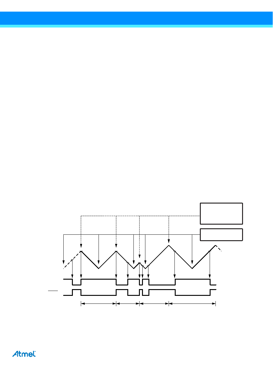
cycle. The timing diagram for the phase correct PWM mode is shown on Figure 13-8. The figure shows phase correct PWM
mode when OCRnA or ICRn is used to define TOP. The TCNTn value is in the timing diagram shown as a histogram for
illustrating the dual-slope operation. The diagram includes non-inverted and inverted PWM outputs. The small horizontal line
marks on the TCNTn slopes represent compare matches between OCRnx and TCNTn. The OCnx Interrupt flag will be set when
a compare match occurs.
Figure 13-8. Phase Correct PWM Mode, Timing Diagram
R
PCPWM
TOP
1
+
()
log
2
()
log
----------------------------------
=
12
3
4
TCNTn
(COMnx1:0 = 2)
(COMnx1:0 = 3)
OCnx
Period
TOVn Interrupt Flag Set
(Interrupt on Bottom)
OCRnx/ TOP Update and
OCnA Interrupt Flag Set
or ICFn Interrupt Flag Set
(Interrupt on TOP)
相關PDF資料 |
PDF描述 |
|---|---|
| M44C090-XXX-DIT | 4-BIT, MROM, 4 MHz, MICROCONTROLLER, UUC |
| M48ST59W-70MH1TR | 0 TIMER(S), REAL TIME CLOCK, PDSO44 |
| M48ST59W-100MH1 | 0 TIMER(S), REAL TIME CLOCK, PDSO44 |
| M48T02-150PC1 | 0 TIMER(S), REAL TIME CLOCK, PDIP24 |
| M48T18-100MH1TR | 0 TIMER(S), REAL TIME CLOCK, PDSO28 |
相關代理商/技術參數(shù) |
參數(shù)描述 |
|---|---|
| M44C890 | 制造商:ATMEL 制造商全稱:ATMEL Corporation 功能描述:Low-Current Microcontroller for Wireless Communication |
| M44C890-H | 制造商:ATMEL 制造商全稱:ATMEL Corporation 功能描述:Low-Current Microcontroller for Wireless Communication |
| M44S05K4F1 | 功能描述:汽車連接器 MX44 Terminals RoHS:否 制造商:Amphenol SINE Systems 產(chǎn)品:Contacts 系列:ATP 位置數(shù)量: 型式:Female 安裝風格: 端接類型: 觸點電鍍:Nickel |
| M44T332538880MHZ | 制造商:MEC 功能描述: |
| M44T3338880MHZ | 制造商:MEC 功能描述: |
發(fā)布緊急采購,3分鐘左右您將得到回復。