- 您現(xiàn)在的位置:買賣IC網(wǎng) > PDF目錄11731 > ORT42G5-1BM484I (Lattice Semiconductor Corporation)IC FPSC TRANSCEIVER 4CH 484-BGA PDF資料下載
參數(shù)資料
| 型號: | ORT42G5-1BM484I |
| 廠商: | Lattice Semiconductor Corporation |
| 文件頁數(shù): | 56/119頁 |
| 文件大小: | 0K |
| 描述: | IC FPSC TRANSCEIVER 4CH 484-BGA |
| 產(chǎn)品變化通告: | Product Discontinuation 01/Aug/2011 |
| 標(biāo)準(zhǔn)包裝: | 60 |
| 系列: | * |
第1頁第2頁第3頁第4頁第5頁第6頁第7頁第8頁第9頁第10頁第11頁第12頁第13頁第14頁第15頁第16頁第17頁第18頁第19頁第20頁第21頁第22頁第23頁第24頁第25頁第26頁第27頁第28頁第29頁第30頁第31頁第32頁第33頁第34頁第35頁第36頁第37頁第38頁第39頁第40頁第41頁第42頁第43頁第44頁第45頁第46頁第47頁第48頁第49頁第50頁第51頁第52頁第53頁第54頁第55頁當(dāng)前第56頁第57頁第58頁第59頁第60頁第61頁第62頁第63頁第64頁第65頁第66頁第67頁第68頁第69頁第70頁第71頁第72頁第73頁第74頁第75頁第76頁第77頁第78頁第79頁第80頁第81頁第82頁第83頁第84頁第85頁第86頁第87頁第88頁第89頁第90頁第91頁第92頁第93頁第94頁第95頁第96頁第97頁第98頁第99頁第100頁第101頁第102頁第103頁第104頁第105頁第106頁第107頁第108頁第109頁第110頁第111頁第112頁第113頁第114頁第115頁第116頁第117頁第118頁第119頁
Lattice Semiconductor
ORCA ORT42G5 and ORT82G5 Data Sheet
41
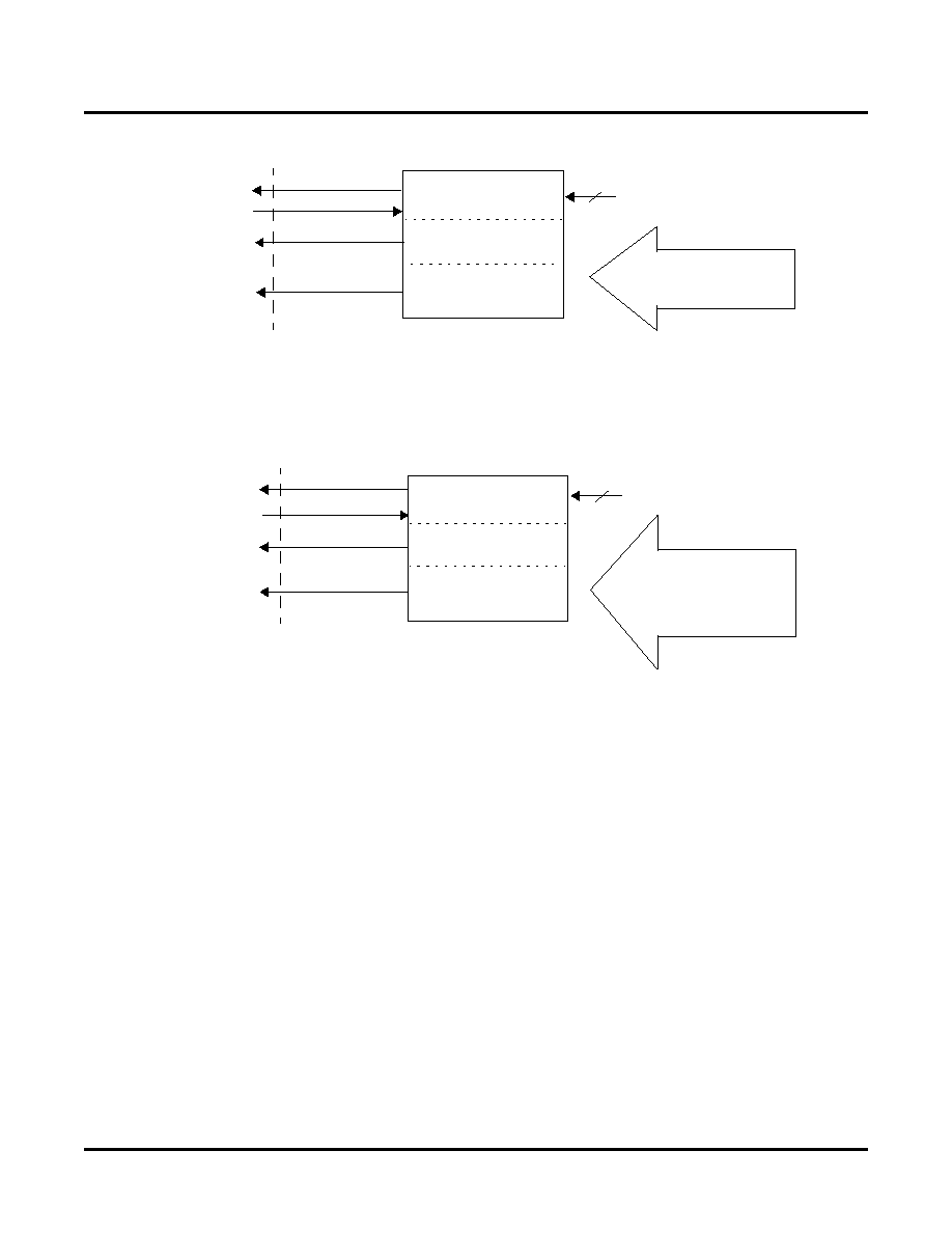
Figure 20. Receive Clocking for a Single Block (Similar Connections Would Be Used for Block B)
The receive channel alignment bypass mode allows mixing of half and full line rates among the channels, as shown
in Figure 21. The gure shows channel AC congured in full rate mode at 2.0 Gbps. Channel AD congured in half-
rate mode at 1.0 Gbps. The receive alignment FIFO per channel cannot be used in this mode.
Figure 21. Receive Clocking for Mixed Line Rates
Each SERDES block can also be congured for any line rate (0.6 to 3.7 Gbps), since each block has its own refer-
ence clock input pins.
Multi-Channel Alignment Clocking Strategies for the ORT42G5
The data on the four channels in the ORT42G5 can be independent of each other or can be synchronized in two
different ways. For example, two channels within a SERDES block can be aligned together, channel C and channel
D. Alternatively, all four channels in a SERDES block can be aligned together to form a communication channel
with a bandwidth of 10 Gbps. Individual channels within an alignment group can be disabled (i.e., powered down)
without disrupting other channels. Clocking strategies for these various modes are described in the following para-
graphs.
For dual alignment both channels must be sourced by the same clock. Either RWCKAC or RWCKAD can be con-
nected to RSYS_CLK_A2. A clocking example for dual alignment is shown in Figure 22.
Common Logic, Block A
Channel AC
Channel AD
REFCLK[P:N]_A
2
156.25 MHz
RCK78A
RWCKAC
RWCKAD
RSYS_CLK_A2
FPGA
Logic
Two Channels of
3.125 Gbps
Incoming Serial Data
78.125 MHz
All Recovered
Clocks at
78.125 MHz
Common Logic, Block A
Channel AC
Channel AD
REFCLK[P:N]_A
2
100 MHz
RCK78A
RWCKAC
FPGA
Logic
One Channel of
2.0 Gbps (Full-Rate)
and One Channel of
1.0 Gbps (Half-Rate)
Incoming Serial Data
25 MHz
RWCKAD
25 MHz
or 50 MHz
50 MHz
RSYS_CLK_A2
相關(guān)PDF資料 |
PDF描述 |
|---|---|
| GRM1885C1H561JA01D | CAP CER 560PF 50V 5% NP0 0603 |
| ORT42G5-1BM484C | IC FPSC TRANSCEIVER 4CH 484-BGA |
| PIC17C43-25/P | IC MCU OTP 4KX16 PWM 40DIP |
| ORSO82G5-2F680I | IC FPSC TRANSCEIVER 8CH 680-BGA |
| ORSO82G5-2F680C | IC FPSC TRANSCEIVER 8CH 680-BGA |
相關(guān)代理商/技術(shù)參數(shù) |
參數(shù)描述 |
|---|---|
| ORT42G5-1BMN484C | 功能描述:FPGA - 現(xiàn)場可編程門陣列 10368 LUT 204 I/O RoHS:否 制造商:Altera Corporation 系列:Cyclone V E 柵極數(shù)量: 邏輯塊數(shù)量:943 內(nèi)嵌式塊RAM - EBR:1956 kbit 輸入/輸出端數(shù)量:128 最大工作頻率:800 MHz 工作電源電壓:1.1 V 最大工作溫度:+ 70 C 安裝風(fēng)格:SMD/SMT 封裝 / 箱體:FBGA-256 |
| ORT42G5-1BMN484I | 功能描述:FPGA - 現(xiàn)場可編程門陣列 10368 LUT 204 I/O RoHS:否 制造商:Altera Corporation 系列:Cyclone V E 柵極數(shù)量: 邏輯塊數(shù)量:943 內(nèi)嵌式塊RAM - EBR:1956 kbit 輸入/輸出端數(shù)量:128 最大工作頻率:800 MHz 工作電源電壓:1.1 V 最大工作溫度:+ 70 C 安裝風(fēng)格:SMD/SMT 封裝 / 箱體:FBGA-256 |
| ORT42G5-2BM484C | 功能描述:FPGA - 現(xiàn)場可編程門陣列 10368 LUT 204 I/O RoHS:否 制造商:Altera Corporation 系列:Cyclone V E 柵極數(shù)量: 邏輯塊數(shù)量:943 內(nèi)嵌式塊RAM - EBR:1956 kbit 輸入/輸出端數(shù)量:128 最大工作頻率:800 MHz 工作電源電壓:1.1 V 最大工作溫度:+ 70 C 安裝風(fēng)格:SMD/SMT 封裝 / 箱體:FBGA-256 |
| ORT42G5-2BM484I | 功能描述:FPGA - 現(xiàn)場可編程門陣列 10368 LUT 204 I/O RoHS:否 制造商:Altera Corporation 系列:Cyclone V E 柵極數(shù)量: 邏輯塊數(shù)量:943 內(nèi)嵌式塊RAM - EBR:1956 kbit 輸入/輸出端數(shù)量:128 最大工作頻率:800 MHz 工作電源電壓:1.1 V 最大工作溫度:+ 70 C 安裝風(fēng)格:SMD/SMT 封裝 / 箱體:FBGA-256 |
| ORT42G5-2BMN484C | 功能描述:FPGA - 現(xiàn)場可編程門陣列 10368 LUT 204 I/O RoHS:否 制造商:Altera Corporation 系列:Cyclone V E 柵極數(shù)量: 邏輯塊數(shù)量:943 內(nèi)嵌式塊RAM - EBR:1956 kbit 輸入/輸出端數(shù)量:128 最大工作頻率:800 MHz 工作電源電壓:1.1 V 最大工作溫度:+ 70 C 安裝風(fēng)格:SMD/SMT 封裝 / 箱體:FBGA-256 |
發(fā)布緊急采購,3分鐘左右您將得到回復(fù)。