- 您現(xiàn)在的位置:買賣IC網(wǎng) > PDF目錄369993 > pentium pro processor (Intel Corp.) Pentium Pro Processor with 1MB L2 Cache at 200MHZ(1兆比特L2高速緩存頻率200兆赫茲處理器) PDF資料下載
參數(shù)資料
| 型號: | pentium pro processor |
| 廠商: | Intel Corp. |
| 英文描述: | Pentium Pro Processor with 1MB L2 Cache at 200MHZ(1兆比特L2高速緩存頻率200兆赫茲處理器) |
| 中文描述: | 奔騰Pro處理器在200MHz(1兆比特二級高速緩存頻率200兆赫茲處理器帶有1MB的L2緩存) |
| 文件頁數(shù): | 11/39頁 |
| 文件大?。?/td> | 930K |
| 代理商: | PENTIUM PRO PROCESSOR |
第1頁第2頁第3頁第4頁第5頁第6頁第7頁第8頁第9頁第10頁當前第11頁第12頁第13頁第14頁第15頁第16頁第17頁第18頁第19頁第20頁第21頁第22頁第23頁第24頁第25頁第26頁第27頁第28頁第29頁第30頁第31頁第32頁第33頁第34頁第35頁第36頁第37頁第38頁第39頁

E
AP-523
11
Vcc
P
L
pin
∞
ESD
Diodes
Package
Boundary
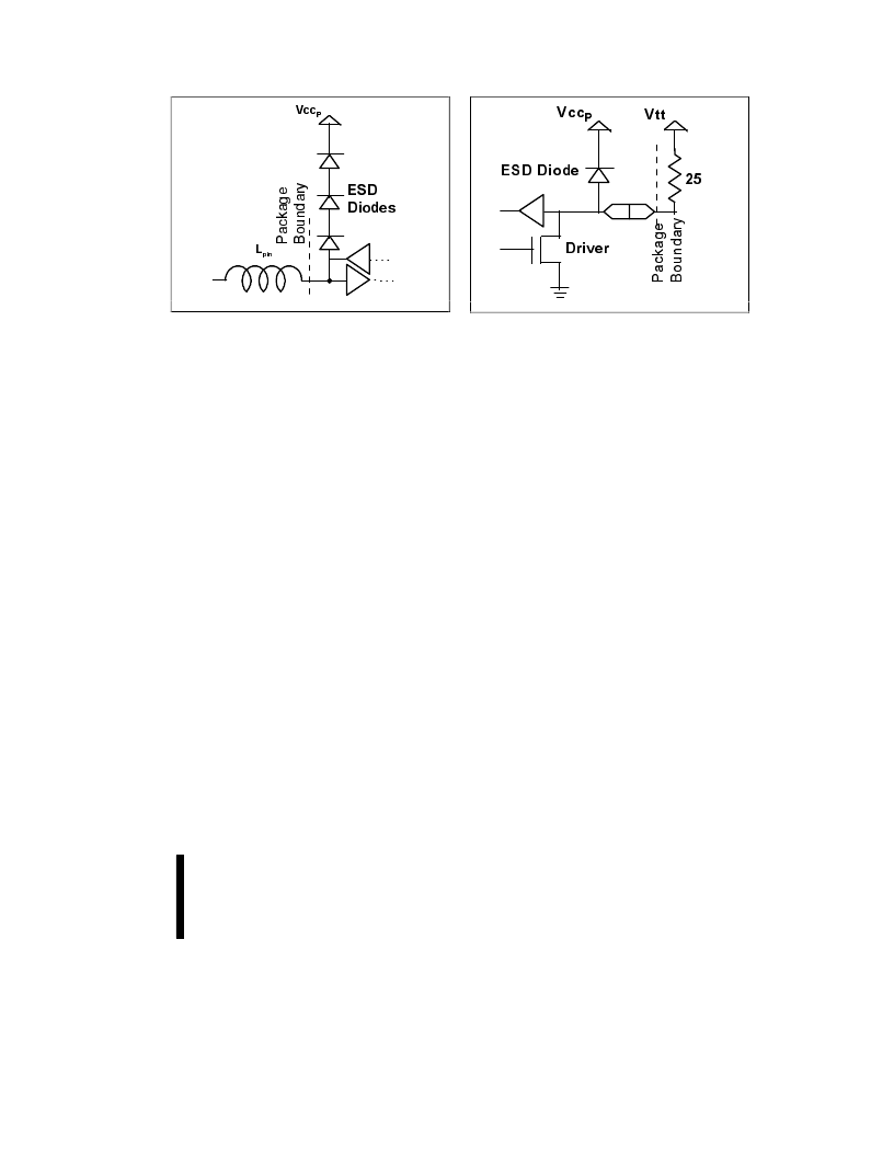
Figure 8. Tolerant ESD Diodes
3.3.1.
3.3V TOLERANT SIGNALS
The 3.3V tolerant buffers are open drain. When the V
CC
P
supply is on, and the 3.3V supply is off, the ESD
protection diodes of the buffers are reverse biased and no
power is supplied to the signal lines. As the processor
sees RESET#, the outputs switch to the high or inactive
state so bus contention after 3.3V comes up is avoided.
If the 3.3V supply is on while the V
CC
P supply is off, the
3.3V supply will deliver current to the Pentium Pro
processor core through the string of three ESD protection
diodes connecting the pads to V
CC
. If a pull-up is used
for the high level of the signals, then 150 ohms will allow
a maximum of only 9 mA of current to be supplied to the
core per pad cell. If the inputs are driven by a CMOS
output, then the current from the output should be limited
to 200 mA maximum output current per Pentium Pro
processor pin.
If V
CC
P is used as the high level for the 3.3V tolerant
signals, then no sequencing issue exists.
3.3.2.
GTL+ SIGNALS
The GTL+ outputs are also open drain. When the V
CC
P
supply is on and V
TT
is off, all inputs appear low and
there will be no current flowing on the GTL+ bus.
If V
TT
is on and V
CC
P is off, the GTL+ bus will attempt
to power up the core through the ESD protection diode.
The resulting V
CC
level will be low enough that no
significant current will be consumed by the core.
25
Vtt
Vcc
P
Driver
∞
ESD Diode
Package
Boundary
Figure 9. GTL+ ESD Diodes
NOTE
Every device on the bus must have power in
order for the GTL+ bus to operate properly.
3.3.3.
MEMORY SIDE SIGNALS
The 5V tolerant signals are internally buffered in a
similar manner. When using 3.3V DRAM there are no
memory side sequencing issues. When the 5V supply is
on to 5V DRAM and the 3.3V memory controller supply
is off, the CAS lines may be floating. This could cause
the DRAM to drive 5V signals to a component that has
no voltage applied. The system should provide weak
pull-ups to 5V on the CAS lines to prevent the 5V
DRAM devices from driving 3.3V inputs when there is
no power to the memory controller.
By providing the memory controller with the
PWRGOOD signal (as described in Section 1.1), it will
drive the CAS lines of the DRAM inactive, and reset the
data buffers as soon as it receives 3.3V. This will hold
the DRAM outputs off and keep the chipset buffer
components in reset during a period of power supply
stabilization. This includes a poor V
TT
that would
prevent the GTL+ bus RESET# signal from being created
correctly. This action protects these devices from
producing bus contention between themselves.
3.3.4.
PCI SIDE SIGNALS
PCI_RST# tells all PCI devices to remain in a tri-state
condition. This signal will be held active by the PCI bus
controller when it is receiving power and its PWR_GD
signal is inactive. The PCI bus controller will also tri-
state its signals during this time. In addition, the PCI
相關PDF資料 |
PDF描述 |
|---|---|
| pentium processor with MMX | 32-bit processor with MMX technology(32位帶MMX技術處理器) |
| pentium processor | 32 Bit Processor With MMX And Mobile Module(32位帶移動模塊和MMX技術CPU) |
| PESD0603-140 | Raychem Overvoltage Devices |
| PESD5V2S18U | ESD protection array |
| PESDXL4UW | Low capacitance quadruple ESD protection array |
相關代理商/技術參數(shù) |
參數(shù)描述 |
|---|---|
| P-ENV568K3G3 | 制造商:Panasonic Industrial Company 功能描述:TUNER |
| PEO14012 | 制造商:TE Connectivity 功能描述:RELAY SPCO 12VDC |
| PEO14024 | 制造商:TE Connectivity 功能描述:RELAY SPCO 24VDC |
| PEO96742 | 制造商:Delphi Corporation 功能描述:ASM TERM |
| PEOODO3A | 制造商:MACOM 制造商全稱:Tyco Electronics 功能描述:Versatile Power Entry Module with Small Footprint |
發(fā)布緊急采購,3分鐘左右您將得到回復。