- 您現(xiàn)在的位置:買賣IC網(wǎng) > PDF目錄192305 > S71GL064A08BAW0F3 (SPANSION LLC) Stacked Multi-Chip Product (MCP) Flash Memory and RAM PDF資料下載
參數(shù)資料
| 型號: | S71GL064A08BAW0F3 |
| 廠商: | SPANSION LLC |
| 元件分類: | 存儲器 |
| 英文描述: | Stacked Multi-Chip Product (MCP) Flash Memory and RAM |
| 中文描述: | SPECIALTY MEMORY CIRCUIT, PBGA56 |
| 封裝: | 7 X 9 MM, 1.20 MM HEIGHT, LEAD FREE, FBGA-56 |
| 文件頁數(shù): | 12/134頁 |
| 文件大小: | 2383K |
| 代理商: | S71GL064A08BAW0F3 |
第1頁第2頁第3頁第4頁第5頁第6頁第7頁第8頁第9頁第10頁第11頁當(dāng)前第12頁第13頁第14頁第15頁第16頁第17頁第18頁第19頁第20頁第21頁第22頁第23頁第24頁第25頁第26頁第27頁第28頁第29頁第30頁第31頁第32頁第33頁第34頁第35頁第36頁第37頁第38頁第39頁第40頁第41頁第42頁第43頁第44頁第45頁第46頁第47頁第48頁第49頁第50頁第51頁第52頁第53頁第54頁第55頁第56頁第57頁第58頁第59頁第60頁第61頁第62頁第63頁第64頁第65頁第66頁第67頁第68頁第69頁第70頁第71頁第72頁第73頁第74頁第75頁第76頁第77頁第78頁第79頁第80頁第81頁第82頁第83頁第84頁第85頁第86頁第87頁第88頁第89頁第90頁第91頁第92頁第93頁第94頁第95頁第96頁第97頁第98頁第99頁第100頁第101頁第102頁第103頁第104頁第105頁第106頁第107頁第108頁第109頁第110頁第111頁第112頁第113頁第114頁第115頁第116頁第117頁第118頁第119頁第120頁第121頁第122頁第123頁第124頁第125頁第126頁第127頁第128頁第129頁第130頁第131頁第132頁第133頁第134頁
February 8, 2005 S71GL064A_00_A2
pSRAM Type 7
107
Adva nc e
inf o r m at ion
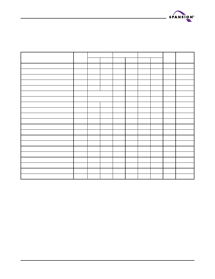
AC Characteristics
(Under Recommended Operating Conditions Unless Otherwise Noted)
Read Operation
Notes:
1. Maximum value is applicable if CE#1 is kept at Low without change of address input of A3 to A21. If needed by system
operation, please contact local Spansion representative for the relaxation of 1s limitation.
2. Address should not be changed within minimum tRC.
3. The output load 50 pF with 50 ohm termination to VDD x 0.5 (16M), The output load 50 pF (32M and 64M).
4. The output load 5pF.
5. Applicable to A3 to A21 (32M and 64M) when CE1# is kept at Low.
6. Applicable only to A0, A1 and A2 (32M and 64M) when CE1# is kept at Low for the page address access.
7. In case Page Read Cycle is continued with keeping CE1# stays Low, CE1# must be brought to High within 4 s. In other
words, Page Read Cycle must be closed within 4 s.
8. Applicable when at least two of address inputs among applicable are switched from previous state.
9. tRC(min) and tPRC(min) must be satisfied.
10. If actual value of tWHOL is shorter than specified minimum values, the actual tAA of following Read can become longer by the
amount of subtracting the actual value from the specified minimum value.
Parameter
Symbol
16M
32M
64M
Unit
Notes
Min.
Max.
Min.
Max.
Min.
Max.
Read Cycle Time
tRC
70
1000
65
1000
65
1000
ns
1, 2
CE1# Access Time
tCE
—60—65
—
65
ns
3
OE# Access Time
tOE
—40—40
—
40
ns
3
Address Access Time
tAA
—60—65
—
65
ns
3, 5
LB# / UB# Access Time
tBA
—30—30
—
30
ns
3
Page Address Access Time
tPAA
N/A
—
20
—
20
ns
3,6
Page Read Cycle Time
tPRC
N/A
20
1000
20
1000
ns
1, 6, 7
Output Data Hold Time
tOH
5
—
5—5—
ns
3
CE1# Low to Output Low-Z
tCLZ
5
—
5—5—
ns
4
OE# Low to Output Low-Z
tOLZ
0
—
0—0—
ns
4
LB# / UB# Low to Output Low-Z
tBLZ
0
—
0—0—
ns
4
CE1# High to Output High-Z
tCHZ
—20—20
—
20
ns
3
OE# High to Output High-Z
tOHZ
—20—14
—
14
ns
3
LB# / UB# High to Output High-Z
tBHZ
—20—20
—
20
ns
3
Address Setup Time to CE1# Low
tASC
6—
–6
—
–6
—
ns
Address Setup Time to OE# Low
tASO
10
—
10
—
10
—
ns
Address Invalid Time
tAX
—10—10
—
10
ns
5, 8
Address Hold Time from CE1# High
tCHAH
-6
—
–6
—
–6
—
ns
9
Address Hold Time from OE# High
tOHAH
-6
—
–6
—
–6
—
ns
WE# High to OE# Low Time for Read
tWHOL
10
1000
12
—
25
—
ns
10
CE1# High Pulse Width
tCP
10
—
12
—
12
—
ns
相關(guān)PDF資料 |
PDF描述 |
|---|---|
| S71GL064A08BFI0B2 | Stacked Multi-Chip Product (MCP) Flash Memory and RAM |
| S71GL064A08BFI0B3 | Stacked Multi-Chip Product (MCP) Flash Memory and RAM |
| S71GL064A08BFI0F3 | Stacked Multi-Chip Product (MCP) Flash Memory and RAM |
| S71GL064A08BFW0B2 | Stacked Multi-Chip Product (MCP) Flash Memory and RAM |
| S71GL064A08BFW0B3 | Stacked Multi-Chip Product (MCP) Flash Memory and RAM |
相關(guān)代理商/技術(shù)參數(shù) |
參數(shù)描述 |
|---|---|
| S71GL064A08BFI0B0 | 制造商:SPANSION 制造商全稱:SPANSION 功能描述:Stacked Multi-Chip Product (MCP) Flash Memory and RAM |
| S71GL064A08BFI0B2 | 制造商:SPANSION 制造商全稱:SPANSION 功能描述:Stacked Multi-Chip Product (MCP) Flash Memory and RAM |
| S71GL064A08BFI0B3 | 制造商:SPANSION 制造商全稱:SPANSION 功能描述:Stacked Multi-Chip Product (MCP) Flash Memory and RAM |
| S71GL064A08BFI0F0 | 制造商:SPANSION 制造商全稱:SPANSION 功能描述:Stacked Multi-Chip Product (MCP) Flash Memory and RAM |
| S71GL064A08BFI0F2 | 制造商:SPANSION 制造商全稱:SPANSION 功能描述:Stacked Multi-Chip Product (MCP) Flash Memory and RAM |
發(fā)布緊急采購,3分鐘左右您將得到回復(fù)。