- 您現(xiàn)在的位置:買賣IC網(wǎng) > PDF目錄8951 > SI5364-H-GL (Silicon Laboratories Inc)IC CLOCK SONET/SDH PORT 99LFBGA PDF資料下載
參數(shù)資料
| 型號: | SI5364-H-GL |
| 廠商: | Silicon Laboratories Inc |
| 文件頁數(shù): | 8/38頁 |
| 文件大?。?/td> | 0K |
| 描述: | IC CLOCK SONET/SDH PORT 99LFBGA |
| 標準包裝: | 168 |
| 系列: | DSPLL® |
| 類型: | 時鐘發(fā)生器,扇出緩沖器(分配) |
| PLL: | 是 |
| 輸入: | 時鐘 |
| 輸出: | CML |
| 電路數(shù): | 1 |
| 比率 - 輸入:輸出: | 3:4 |
| 差分 - 輸入:輸出: | 是/是 |
| 頻率 - 最大: | 675MHz |
| 除法器/乘法器: | 無/是 |
| 電源電壓: | 3.135 V ~ 3.465 V |
| 工作溫度: | -20°C ~ 85°C |
| 安裝類型: | 表面貼裝 |
| 封裝/外殼: | 99-LBGA |
| 供應商設備封裝: | 99-BGA(11x11) |
| 包裝: | 托盤 |
第1頁第2頁第3頁第4頁第5頁第6頁第7頁當前第8頁第9頁第10頁第11頁第12頁第13頁第14頁第15頁第16頁第17頁第18頁第19頁第20頁第21頁第22頁第23頁第24頁第25頁第26頁第27頁第28頁第29頁第30頁第31頁第32頁第33頁第34頁第35頁第36頁第37頁第38頁
Si5364
16
Rev. 2.5
2.1.1. FEC Rate Conversion
Conversion from non-FEC to FEC rates and from FEC
to non-FEC rates is supported with selectable 238/255
or 255/238 scaling of the Si5364’s clock output
multiplication ratios.
The multiplication ratios and associated frequency
ranges for the Si5364 clock outputs are set by the
FRQSEL[1:0] pins associated with each clock output.
Additional frequency scaling of active clock outputs by a
factor of either 238/255 or 255/238 is selected using the
FEC[1:0] control inputs.
For example, a 622.08 MHz output clock (a non-FEC
rate) is generated from a 19.44 MHz input clock (a non-
FEC
rate)
by
setting
FRQSEL[1:0] = 11
(32x
multiplication) and setting FEC[1:0] = 00 (no FEC
scaling). A 666.51 MHz output clock (a FEC rate) is
generated from a 19.44 MHz input clock (a non-FEC
rate) by setting FRQSEL[1:0] = 11 (32x multiplication)
and setting FEC[1:0] = 01 (255/238 FEC scaling).
Finally, a 622.08 MHz output clock (a non-FEC rate) is
generated from a 20.83 MHz input clock (a FEC rate) by
setting FRQSEL [1:0] = 11 (32x multiplication) and
setting FEC[1:0] = 10 (238/255 FEC scaling). The
FEC[1:0] settings and associated scaling factors are
listed in Table 9.
2.2. PLL Performance
The Si5364 PLL provides extremely low jitter
generation, high jitter tolerance, and a well-controlled
jitter transfer function with low peaking and a high
degree of jitter attenuation. Each of these key
performance parameters is described in the following
sections.
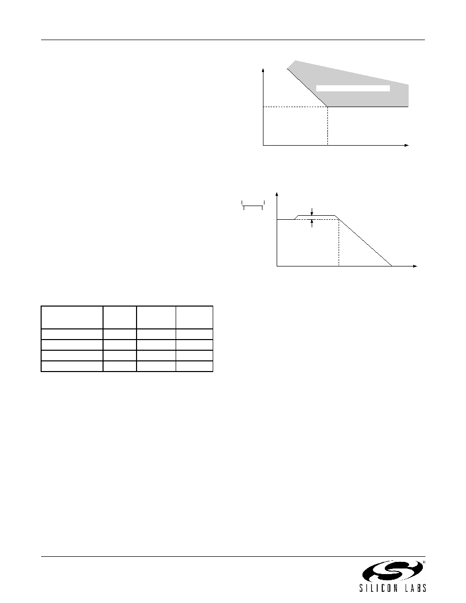
2.2.1. Jitter Tolerance
Jitter tolerance for the Si5364 is defined as the
maximum peak-to-peak sinusoidal jitter that can be
present on the incoming clock. Tolerance is a function of
the input jitter frequency and improves for lower input
jitter frequency.
Figure 8. Jitter Tolerance Mask/Template
Figure 9. PLL Jitter Transfer Mask/Template
2.2.2. Jitter Transfer
Jitter transfer is defined as the ratio of output signal jitter
to input signal jitter for a specified jitter frequency. The
jitter transfer characteristic determines the amount of
input clock jitter that passes to the outputs. The DSPLL
technology used in the Si5364 provides tightly
controlled jitter transfer curves because the PLL gain
parameters are determined by digital circuits that do not
vary over supply voltage, process, and temperature. In
a system application, a well-controlled transfer curve
minimizes the output clock jitter variation from board to
board for consistent system-level jitter performance.
The jitter transfer characteristic is a function of the
BWSEL[1:0] setting. Lower bandwidth selection results
in more jitter attenuation of the incoming clock but might
result in higher jitter generation. Table 4 on page 9 gives
the 3 dB bandwidth and peaking values for specified
BWSEL[1:0] settings. Figure 9 shows the jitter transfer
curve mask.
2.2.3. Jitter Generation
Jitter generation is defined as the amount of jitter
produced at the output of the device with a jitter-free
input clock. Jitter is generated from sources within the
VCO and other PLL components. Jitter generation is a
function of the PLL bandwidth setting.
Table 9. FEC Rate Conversion
FEC Frequency
Scaling
FEC1
FEC0
FSYNC
1/1
0
Enabled
255/238
0
1
Disabled
238/255
1
0
Enabled
Reserved
1
Input
Jitter
Amplitude
10 ns
F
BW
–20 dB/dec.
f
Jitter In
Excessive Input Jitter Range
Jitter
Transfer
0 dB
F
BW
f
Jitter
Peaking
–20 dB/dec.
Jitter Out
Jitter In
(s)
相關PDF資料 |
PDF描述 |
|---|---|
| VE-26H-MW-F4 | CONVERTER MOD DC/DC 52V 100W |
| SI5321-H-GL | IC CLOCK MULT SONET/SDH 63LFBGA |
| VE-JVJ-MZ-F3 | CONVERTER MOD DC/DC 36V 25W |
| VE-26H-MW-F2 | CONVERTER MOD DC/DC 52V 100W |
| VE-26H-MW-F1 | CONVERTER MOD DC/DC 52V 100W |
相關代理商/技術參數(shù) |
參數(shù)描述 |
|---|---|
| Si5364-H-GLR | 功能描述:時鐘發(fā)生器及支持產(chǎn)品 SONET/SDH Precision 19MHz 155MHz 622MHz RoHS:否 制造商:Silicon Labs 類型:Clock Generators 最大輸入頻率:14.318 MHz 最大輸出頻率:166 MHz 輸出端數(shù)量:16 占空比 - 最大:55 % 工作電源電壓:3.3 V 工作電源電流:1 mA 最大工作溫度:+ 85 C 安裝風格:SMD/SMT 封裝 / 箱體:QFN-56 |
| SI5365 | 制造商:SILABS 制造商全稱:SILABS 功能描述:PIN-PROGRAMMABLE PRECISION CLOCK MULTIPLIER |
| Si5365/66-EVB | 功能描述:時鐘和定時器開發(fā)工具 Si5365/Si5366 EVAL BOARD RoHS:否 制造商:Texas Instruments 產(chǎn)品:Evaluation Modules 類型:Clock Conditioners 工具用于評估:LMK04100B 頻率:122.8 MHz 工作電源電壓:3.3 V |
| Si5365-B-GQ | 功能描述:時鐘合成器/抖動清除器 PIN-PROGRAMMABLE CLK MULTIPLIER 5 OUTS RoHS:否 制造商:Skyworks Solutions, Inc. 輸出端數(shù)量: 輸出電平: 最大輸出頻率: 輸入電平: 最大輸入頻率:6.1 GHz 電源電壓-最大:3.3 V 電源電壓-最小:2.7 V 封裝 / 箱體:TSSOP-28 封裝:Reel |
| SI5365-B-GQR | 制造商:Silicon Laboratories Inc 功能描述: |
發(fā)布緊急采購,3分鐘左右您將得到回復。