- 您現(xiàn)在的位置:買賣IC網(wǎng) > PDF目錄385876 > STPCCONSUMER-S (意法半導(dǎo)體) CONNECTOR ACCESSORY PDF資料下載
參數(shù)資料
| 型號(hào): | STPCCONSUMER-S |
| 廠商: | 意法半導(dǎo)體 |
| 英文描述: | CONNECTOR ACCESSORY |
| 中文描述: | 連接器附件 |
| 文件頁數(shù): | 29/51頁 |
| 文件大小: | 836K |
| 代理商: | STPCCONSUMER-S |
第1頁第2頁第3頁第4頁第5頁第6頁第7頁第8頁第9頁第10頁第11頁第12頁第13頁第14頁第15頁第16頁第17頁第18頁第19頁第20頁第21頁第22頁第23頁第24頁第25頁第26頁第27頁第28頁當(dāng)前第29頁第30頁第31頁第32頁第33頁第34頁第35頁第36頁第37頁第38頁第39頁第40頁第41頁第42頁第43頁第44頁第45頁第46頁第47頁第48頁第49頁第50頁第51頁
ELECTRICAL SPECIFICATIONS
29/51
Release B
This is preliminary information on a new product now in development or undergoing evaluation. Details are subject to change without notice.
4.1 DC Characteristics
Notes:
1. MHz ratings refer to CPU clock frequency.
2. Not 100% tested.
4.1 AC Characteristics
Table 4.4 through Table 4.9 list the AC character-
istics including output delays, input setup require-
ments, input hold requirements and output float
delays. These measurements are based on the
measurement points identified in Figure 4.1. The
rising clock edge reference level VREF , and other
reference levels are shown in Table 4.3 below for
the STPC Consumer-S. Input or output signals
must cross these levels during testing.
Figure 4.1 shows output delay (A and B) and input
setup and hold times (C and D). Input setup and
hold times (C and D) are specified minimums, de-
fining the smallest acceptable sampling window a
synchronous input signal must be stable for cor-
rect operation.
Note: Refer to Figure 4.1.
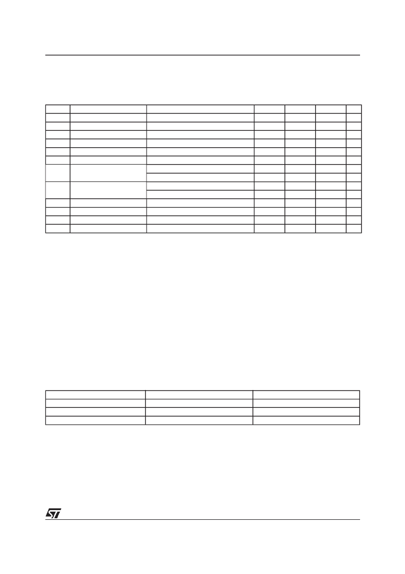
Table 4.2. DC Characteristics
Recommended Operating conditions : VDD = 3.3V
±
0.3V, Tcase = 0 to 100
°
C unless otherwise specified
Symbol
V
DD
P
DD
H
CLK
V
REF
V
OL
V
OH
V
IL
Parameter
Test conditions
Min
3.0
Typ
3.3
3.2
Max
3.6
3.9
75
1.255
0.5
Unit
V
W
Mhz
V
V
V
V
V
V
V
μ
A
pF
pF
pF
Operating Voltage
Supply Power
Internal Clock
DAC Voltage Reference
Output Low Voltage
Output High Voltage
Input Low Voltage
V
DD
= 3.3V, H
CLK
= 66Mhz
(Note 1)
1.215
1.235
I
Load
=1.5 to 8mA depending of the pin
I
Load
=-0.5 to -8mA depending of the pin
Except XTALI
XTALI
Except XTALI
XTALI
Input, I/O
(Note 2)
(Note 2)
(Note 2)
2.4
-0.3
-0.3
2.1
2.35
-5
0.8
0.9
V
IH
Input High Voltage
V
DD
+0.3
V
DD
+0.3
5
I
LK
C
IN
C
OUT
C
CLK
Input Leakage Current
Input Capacitance
Output Capacitance
Clock Capacitance
Table 4.3. Drive Level and Measurement Points for Switching Characteristics
Symbol
V
REF
V
IHD
V
ILD
Value
1.5
3.0
0.0
Units
V
V
V
相關(guān)PDF資料 |
PDF描述 |
|---|---|
| STPCI0166BTC3 | PC Compatible Embedded Microprocessor |
| STPCINDUSTRIAL | PC Compatible Embedded Microprocessor |
| STPCI0180BTC3 | PC Compatible Embedded Microprocessor |
| STPCI0180BTI3 | PC Compatible Embedded Microprocessor |
| STPCI0166BTI3 | PC Compatible Embedded Microprocessor |
相關(guān)代理商/技術(shù)參數(shù) |
參數(shù)描述 |
|---|---|
| STPCD01 | 制造商:未知廠家 制造商全稱:未知廠家 功能描述:STPC CLIENT DATASHEET / PC COMPATIBLE EMBEDED MICROPROCESSOR |
| STPCD0110BTC3 | 制造商:未知廠家 制造商全稱:未知廠家 功能描述:32-Bit Microprocessor |
| STPCD0112BTC3 | 制造商:未知廠家 制造商全稱:未知廠家 功能描述:32-Bit Microprocessor |
| STPCD0113BTC3 | 制造商:未知廠家 制造商全稱:未知廠家 功能描述:32-Bit Microprocessor |
| STPCD0166BTA3 | 制造商:STMICROELECTRONICS 制造商全稱:STMicroelectronics 功能描述:PC Compatible Embedded Microprocessor |
發(fā)布緊急采購(gòu),3分鐘左右您將得到回復(fù)。