- 您現(xiàn)在的位置:買賣IC網(wǎng) > PDF目錄225277 > T431616D (Electronic Theatre Controls, Inc.) 1M x 16 SDRAM 512K x 16bit x 2Banks Synchronous DRAM PDF資料下載
參數(shù)資料
| 型號: | T431616D |
| 廠商: | Electronic Theatre Controls, Inc. |
| 英文描述: | 1M x 16 SDRAM 512K x 16bit x 2Banks Synchronous DRAM |
| 中文描述: | 100萬× 16內(nèi)存為512k × 16Bit的X 2Banks同步DRAM |
| 文件頁數(shù): | 3/74頁 |
| 文件大?。?/td> | 781K |
| 代理商: | T431616D |
第1頁第2頁當(dāng)前第3頁第4頁第5頁第6頁第7頁第8頁第9頁第10頁第11頁第12頁第13頁第14頁第15頁第16頁第17頁第18頁第19頁第20頁第21頁第22頁第23頁第24頁第25頁第26頁第27頁第28頁第29頁第30頁第31頁第32頁第33頁第34頁第35頁第36頁第37頁第38頁第39頁第40頁第41頁第42頁第43頁第44頁第45頁第46頁第47頁第48頁第49頁第50頁第51頁第52頁第53頁第54頁第55頁第56頁第57頁第58頁第59頁第60頁第61頁第62頁第63頁第64頁第65頁第66頁第67頁第68頁第69頁第70頁第71頁第72頁第73頁第74頁
TE
CH
tm
T431616D/E
TM Technology Inc. reserves the right
P. 11
Publication Date: FEB. 2007
to change products or specifications without notice.
Revision: A
6
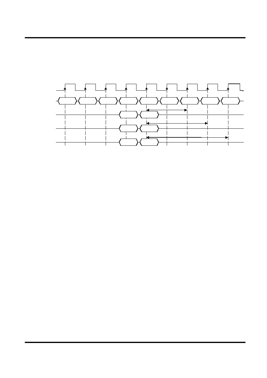
Write and AutoPrecharge command (refer to the following figure)
(RAS# = "H", CAS# = "L", WE# = "L", A11 = “V”, A10 = "H", A0-A7 = Column Address)
The Write and AutoPrecharge command performs the precharge operation automatically after the write
operation. Once this command is given, any subsequent command can not occur within a time delay of {(burst
length -1) + tWR + tRP(min.)}. At full-page burst, only the write operation is performed in this command and the
auto precharge function is ignored.
CLK
COMM AND
T0
T1
T2T3
T4T5
T6T7
T8
NOP
DIN A0
DIN A1
CAS# latency=1
tCK1, DQ's
CAS# latency=2
tCK2, DQ's
CAS# latency=3
tCK3, DQ's
DIN A0
DIN A1
DIN A0
DIN A1
tDAL
*
tDAL= tWR + tRP
* Begin AutoPrecharge
Bank can be reactivated at completion of
tDAL
Bank A
Activate
Write A
AutoPrecharge
tDAL
Burst Write with Auto-Precharge (Burst Length = 2, CAS# Latency = 1, 2, 3)
7
Mode Register Set command
(RAS# = "L", CAS# = "L", WE# = "L", A11 = “V”, A10 = “V”, A0-A9 = Register Data)
The mode register stores the data for controlling the various operating modes of SDRAM. The Mode
Register Set command programs the values of CAS# latency, Addressing Mode and Burst Length in the Mode
register to make SDRAM useful for a variety of different applications. The default values of the Mode Register
after power-up are undefined; therefore this command must be issued at the power-up sequence. The state of pins
A0~A9 and A11 in the same cycle is the data written to the mode register. One clock cycle is required to
complete the write in the mode register (refer to the following figure). The contents of the mode register can be
changed using the same command and the clock cycle requirements during operation as long as both banks are in
the idle state.
相關(guān)PDF資料 |
PDF描述 |
|---|---|
| T431616E | 1M x 16 SDRAM 512K x 16bit x 2Banks Synchronous DRAM |
| T450N | 0 MHz - 10000 MHz 50 ohm RF/MICROWAVE TERMINATION |
| T451N | 0 MHz - 10000 MHz 50 ohm RF/MICROWAVE TERMINATION |
| T523-020.00M | TCXO, CLIPPED SINE OUTPUT, 20 MHz |
| T613-020.00M | TCXO, CLIPPED SINE OUTPUT, 20 MHz |
相關(guān)代理商/技術(shù)參數(shù) |
參數(shù)描述 |
|---|---|
| T431616D-5C | 制造商:TMT 制造商全稱:TMT 功能描述:1M x 16 SDRAM 512K x 16bit x 2Banks Synchronous DRAM |
| T431616D-5CG | 制造商:TMT 制造商全稱:TMT 功能描述:1M x 16 SDRAM 512K x 16bit x 2Banks Synchronous DRAM |
| T431616D-5S | 制造商:TMT 制造商全稱:TMT 功能描述:1M x 16 SDRAM 512K x 16bit x 2Banks Synchronous DRAM |
| T431616D-5SG | 制造商:TMT 制造商全稱:TMT 功能描述:1M x 16 SDRAM 512K x 16bit x 2Banks Synchronous DRAM |
| T431616D-6C | 制造商:TMT 制造商全稱:TMT 功能描述:1M x 16 SDRAM 512K x 16bit x 2Banks Synchronous DRAM |
發(fā)布緊急采購,3分鐘左右您將得到回復(fù)。