- 您現(xiàn)在的位置:買賣IC網(wǎng) > PDF目錄272328 > T83C154DXXX-20 (TEMIC SEMICONDUCTORS) 8-BIT, MROM, 20 MHz, MICROCONTROLLER, PQFP44 PDF資料下載
參數(shù)資料
| 型號: | T83C154DXXX-20 |
| 廠商: | TEMIC SEMICONDUCTORS |
| 元件分類: | 微控制器/微處理器 |
| 英文描述: | 8-BIT, MROM, 20 MHz, MICROCONTROLLER, PQFP44 |
| 文件頁數(shù): | 17/242頁 |
| 文件大小: | 3080K |
| 代理商: | T83C154DXXX-20 |
第1頁第2頁第3頁第4頁第5頁第6頁第7頁第8頁第9頁第10頁第11頁第12頁第13頁第14頁第15頁第16頁當(dāng)前第17頁第18頁第19頁第20頁第21頁第22頁第23頁第24頁第25頁第26頁第27頁第28頁第29頁第30頁第31頁第32頁第33頁第34頁第35頁第36頁第37頁第38頁第39頁第40頁第41頁第42頁第43頁第44頁第45頁第46頁第47頁第48頁第49頁第50頁第51頁第52頁第53頁第54頁第55頁第56頁第57頁第58頁第59頁第60頁第61頁第62頁第63頁第64頁第65頁第66頁第67頁第68頁第69頁第70頁第71頁第72頁第73頁第74頁第75頁第76頁第77頁第78頁第79頁第80頁第81頁第82頁第83頁第84頁第85頁第86頁第87頁第88頁第89頁第90頁第91頁第92頁第93頁第94頁第95頁第96頁第97頁第98頁第99頁第100頁第101頁第102頁第103頁第104頁第105頁第106頁第107頁第108頁第109頁第110頁第111頁第112頁第113頁第114頁第115頁第116頁第117頁第118頁第119頁第120頁第121頁第122頁第123頁第124頁第125頁第126頁第127頁第128頁第129頁第130頁第131頁第132頁第133頁第134頁第135頁第136頁第137頁第138頁第139頁第140頁第141頁第142頁第143頁第144頁第145頁第146頁第147頁第148頁第149頁第150頁第151頁第152頁第153頁第154頁第155頁第156頁第157頁第158頁第159頁第160頁第161頁第162頁第163頁第164頁第165頁第166頁第167頁第168頁第169頁第170頁第171頁第172頁第173頁第174頁第175頁第176頁第177頁第178頁第179頁第180頁第181頁第182頁第183頁第184頁第185頁第186頁第187頁第188頁第189頁第190頁第191頁第192頁第193頁第194頁第195頁第196頁第197頁第198頁第199頁第200頁第201頁第202頁第203頁第204頁第205頁第206頁第207頁第208頁第209頁第210頁第211頁第212頁第213頁第214頁第215頁第216頁第217頁第218頁第219頁第220頁第221頁第222頁第223頁第224頁第225頁第226頁第227頁第228頁第229頁第230頁第231頁第232頁第233頁第234頁第235頁第236頁第237頁第238頁第239頁第240頁第241頁第242頁
113
2588F–AVR–06/2013
ATtiny261/461/861
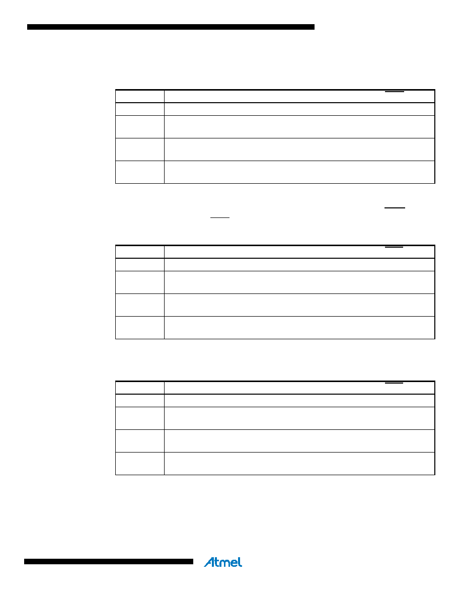
Table 12-10 shows the COM1A1:0 bit functionality when the PWM1A, WGM10 and WGM11 bits
are set to Phase and Frequency Correct PWM Mode.
Table 12-11 shows the COM1A1:0 bit functionality when the PWM1A, WGM10 and WGM11 bits
are set to single-slope PWM6 Mode. In the PWM6 Mode the same Waveform Output (OCW1A)
is used for generating all waveforms and the Output Compare values OC1A and OC1A are con-
nected on thw all OC1x and OC1x pins as described below.
Table 12-12 shows the COM1A1:0 bit functionality when the PWM1A, WGM10 and WGM11 bits
are set to dual-slope PWM6 Mode.I
Bits COM1A1 and COM1A0 are shadowed in TCCR1C. Writing to bits COM1A1 and COM1A0
will also change bits COM1A1S and COM1A0S in TCCR1C. Similary, changes written to bits
COM1A1S and COM1A0S in TCCR1C will show here. See “TCCR1C – Timer/Counter1 Control
Table 12-10. Compare Output Mode, Phase and Frequency Correct PWM Mode
COM1A1:0
OCW1A Behaviour
OC1A Pin
00
Normal port operation.
Disconnected
01
Cleared on Compare Match when up-counting.
Set on Compare Match when down-counting.
Connected
10
Cleared on Compare Match when up-counting.
Set on Compare Match when down-counting.
Connected
Disconnected
11
Set on Compare Match when up-counting.
Cleared on Compare Match when down-counting.
Connected
Disconnected
Table 12-11. Compare Output Mode, Single-Slope PWM6 Mode
COM1A1:0
OCW1A Behaviour
OC1x Pin
00
Normal port operation.
Disconnected
01
Cleared on Compare Match.
Set when TCNT1 = 0x000.
OC1A
10
Cleared on Compare Match.
Set when TCNT1 = 0x000.
OC1A
11
Set on Compare Match.
Cleared when TCNT1 = 0x000.
OC1A
Table 12-12. Compare Output Mode, Dual-Slope PWM6 Mode
COM1A1:0
OCW1A Behaviour
OC1x Pin
00
Normal port operation.
Disconnected
01
Cleared on Compare Match when up-counting.
Set on Compare Match when down-counting.
OC1A
10
Cleared on Compare Match when up-counting.
Set on Compare Match when down-counting.
OC1A
11
Set on Compare Match when up-counting.
Cleared on Compare Match when down-counting.
OC1A
相關(guān)PDF資料 |
PDF描述 |
|---|---|
| TA80486DX2-50 | 32-BIT, 50 MHz, MICROPROCESSOR, CPGA168 |
| T80C32U-S:D | 8-BIT, 20 MHz, MICROCONTROLLER, PQFP44 |
| T83C154DUFXXX-30:R | 8-BIT, MROM, 30 MHz, MICROCONTROLLER, PQFP44 |
| TN83C51GB | 8-BIT, MROM, 6 MHz, MICROCONTROLLER, PQCC68 |
| TS(X)PC603EMAB/C4LN | 32-BIT, 120 MHz, RISC PROCESSOR, CQFP240 |
相關(guān)代理商/技術(shù)參數(shù) |
參數(shù)描述 |
|---|---|
| T83C154-L16 | 制造商:未知廠家 制造商全稱:未知廠家 功能描述:8-Bit Microcontroller |
| T83C154T-12 | 制造商:未知廠家 制造商全稱:未知廠家 功能描述:8-Bit Microcontroller |
| T83C154T-16 | 制造商:未知廠家 制造商全稱:未知廠家 功能描述:8-Bit Microcontroller |
| T83C154T-20 | 制造商:未知廠家 制造商全稱:未知廠家 功能描述:8-Bit Microcontroller |
| T83C154T-25 | 制造商:未知廠家 制造商全稱:未知廠家 功能描述:8-Bit Microcontroller |
發(fā)布緊急采購,3分鐘左右您將得到回復(fù)。