- 您現(xiàn)在的位置:買賣IC網(wǎng) > PDF目錄272328 > T83C154DXXX-20 (TEMIC SEMICONDUCTORS) 8-BIT, MROM, 20 MHz, MICROCONTROLLER, PQFP44 PDF資料下載
參數(shù)資料
| 型號(hào): | T83C154DXXX-20 |
| 廠商: | TEMIC SEMICONDUCTORS |
| 元件分類: | 微控制器/微處理器 |
| 英文描述: | 8-BIT, MROM, 20 MHz, MICROCONTROLLER, PQFP44 |
| 文件頁數(shù): | 222/242頁 |
| 文件大小: | 3080K |
| 代理商: | T83C154DXXX-20 |
第1頁第2頁第3頁第4頁第5頁第6頁第7頁第8頁第9頁第10頁第11頁第12頁第13頁第14頁第15頁第16頁第17頁第18頁第19頁第20頁第21頁第22頁第23頁第24頁第25頁第26頁第27頁第28頁第29頁第30頁第31頁第32頁第33頁第34頁第35頁第36頁第37頁第38頁第39頁第40頁第41頁第42頁第43頁第44頁第45頁第46頁第47頁第48頁第49頁第50頁第51頁第52頁第53頁第54頁第55頁第56頁第57頁第58頁第59頁第60頁第61頁第62頁第63頁第64頁第65頁第66頁第67頁第68頁第69頁第70頁第71頁第72頁第73頁第74頁第75頁第76頁第77頁第78頁第79頁第80頁第81頁第82頁第83頁第84頁第85頁第86頁第87頁第88頁第89頁第90頁第91頁第92頁第93頁第94頁第95頁第96頁第97頁第98頁第99頁第100頁第101頁第102頁第103頁第104頁第105頁第106頁第107頁第108頁第109頁第110頁第111頁第112頁第113頁第114頁第115頁第116頁第117頁第118頁第119頁第120頁第121頁第122頁第123頁第124頁第125頁第126頁第127頁第128頁第129頁第130頁第131頁第132頁第133頁第134頁第135頁第136頁第137頁第138頁第139頁第140頁第141頁第142頁第143頁第144頁第145頁第146頁第147頁第148頁第149頁第150頁第151頁第152頁第153頁第154頁第155頁第156頁第157頁第158頁第159頁第160頁第161頁第162頁第163頁第164頁第165頁第166頁第167頁第168頁第169頁第170頁第171頁第172頁第173頁第174頁第175頁第176頁第177頁第178頁第179頁第180頁第181頁第182頁第183頁第184頁第185頁第186頁第187頁第188頁第189頁第190頁第191頁第192頁第193頁第194頁第195頁第196頁第197頁第198頁第199頁第200頁第201頁第202頁第203頁第204頁第205頁第206頁第207頁第208頁第209頁第210頁第211頁第212頁第213頁第214頁第215頁第216頁第217頁第218頁第219頁第220頁第221頁當(dāng)前第222頁第223頁第224頁第225頁第226頁第227頁第228頁第229頁第230頁第231頁第232頁第233頁第234頁第235頁第236頁第237頁第238頁第239頁第240頁第241頁第242頁
80
2588F–AVR–06/2013
ATtiny261/461/861
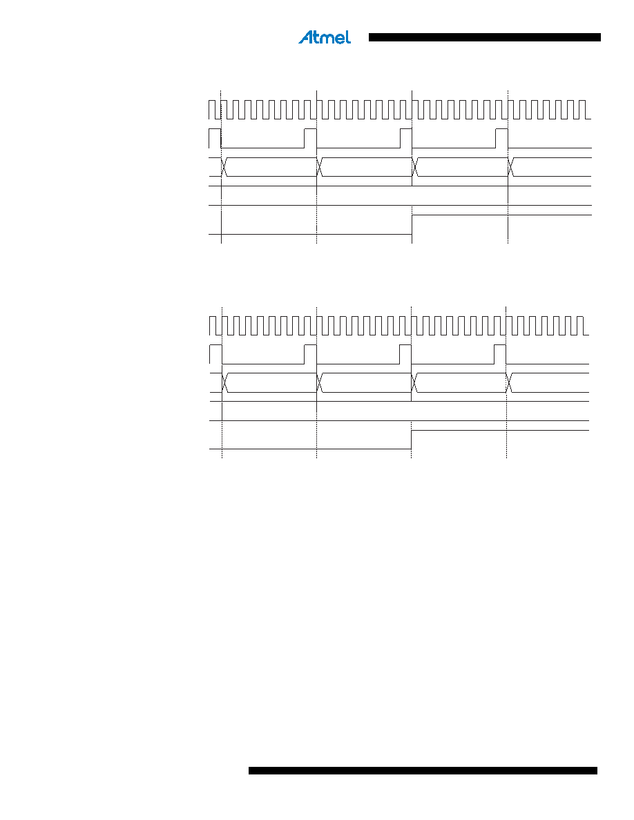
Figure 11-9.
Timer/Counter Timing Diagram, Setting of OCF0x, with Prescaler (f
clk_I/O/8)
Figure 11-10 shows the setting of OCF0A and the clearing of TCNT0 in CTC mode.
Figure 11-10. Timer/Counter Timing Diagram, CTC mode, with Prescaler (f
clk_I/O/8)
11.9
Accessing Registers in 16-bit Mode
In 16-bit mode (the TCW0 bit is set to one) the TCNT0H/L and OCR0A/B or TCNT0L/H and
OCR0B/A are 16-bit registers that can be accessed by the AVR CPU via the 8-bit data bus. The
16-bit register must be byte accessed using two read or write operations. The 16-bit
Timer/Counter has a single 8-bit register for temporary storing of the high byte of the 16-bit
access. The same temporary register is shared between all 16-bit registers. Accessing the low
byte triggers the 16-bit read or write operation. When the low byte of a 16-bit register is written
by the CPU, the high byte stored in the temporary register, and the low byte written are both cop-
ied into the 16-bit register in the same clock cycle. When the low byte of a 16-bit register is read
by the CPU, the high byte of the 16-bit register is copied into the temporary register in the same
clock cycle as the low byte is read.
There is one exception in the temporary register usage. In the Output Compare mode the 16-bit
Output Compare Register OCR0A/B is read without the temporary register, because the Output
Compare Register contains a fixed value that is only changed by CPU access. However, in 16-
bit Input Capture mode the ICR0 register formed by the OCR0A and OCR0B registers must be
accessed with the temporary register.
To do a 16-bit write, the high byte must be written before the low byte. For a 16-bit read, the low
byte must be read before the high byte.
OCFnx
OCRnx
TCNTn
OCRnx Value
OCRnx - 1
OCRnx
OCRnx + 1
OCRnx + 2
clk
I/O
clk
Tn
(clk
I/O/8)
OCFnx
OCRnx
TCNTn
(CTC)
TOP
TOP - 1
TOP
BOTTOM
BOTTOM + 1
clk
PCK
clk
Tn
(clk
PCK /8)
相關(guān)PDF資料 |
PDF描述 |
|---|---|
| TA80486DX2-50 | 32-BIT, 50 MHz, MICROPROCESSOR, CPGA168 |
| T80C32U-S:D | 8-BIT, 20 MHz, MICROCONTROLLER, PQFP44 |
| T83C154DUFXXX-30:R | 8-BIT, MROM, 30 MHz, MICROCONTROLLER, PQFP44 |
| TN83C51GB | 8-BIT, MROM, 6 MHz, MICROCONTROLLER, PQCC68 |
| TS(X)PC603EMAB/C4LN | 32-BIT, 120 MHz, RISC PROCESSOR, CQFP240 |
相關(guān)代理商/技術(shù)參數(shù) |
參數(shù)描述 |
|---|---|
| T83C154-L16 | 制造商:未知廠家 制造商全稱:未知廠家 功能描述:8-Bit Microcontroller |
| T83C154T-12 | 制造商:未知廠家 制造商全稱:未知廠家 功能描述:8-Bit Microcontroller |
| T83C154T-16 | 制造商:未知廠家 制造商全稱:未知廠家 功能描述:8-Bit Microcontroller |
| T83C154T-20 | 制造商:未知廠家 制造商全稱:未知廠家 功能描述:8-Bit Microcontroller |
| T83C154T-25 | 制造商:未知廠家 制造商全稱:未知廠家 功能描述:8-Bit Microcontroller |
發(fā)布緊急采購,3分鐘左右您將得到回復(fù)。