- 您現(xiàn)在的位置:買(mǎi)賣(mài)IC網(wǎng) > PDF目錄385899 > TAS5036IPFCR (Texas Instruments, Inc.) SIX CHANNEL DIGITAL AUDIO PWM PROCESSOR PDF資料下載
參數(shù)資料
| 型號(hào): | TAS5036IPFCR |
| 廠商: | Texas Instruments, Inc. |
| 英文描述: | SIX CHANNEL DIGITAL AUDIO PWM PROCESSOR |
| 中文描述: | 六聲道數(shù)字音頻PWM處理器 |
| 文件頁(yè)數(shù): | 25/49頁(yè) |
| 文件大?。?/td> | 642K |
| 代理商: | TAS5036IPFCR |
第1頁(yè)第2頁(yè)第3頁(yè)第4頁(yè)第5頁(yè)第6頁(yè)第7頁(yè)第8頁(yè)第9頁(yè)第10頁(yè)第11頁(yè)第12頁(yè)第13頁(yè)第14頁(yè)第15頁(yè)第16頁(yè)第17頁(yè)第18頁(yè)第19頁(yè)第20頁(yè)第21頁(yè)第22頁(yè)第23頁(yè)第24頁(yè)當(dāng)前第25頁(yè)第26頁(yè)第27頁(yè)第28頁(yè)第29頁(yè)第30頁(yè)第31頁(yè)第32頁(yè)第33頁(yè)第34頁(yè)第35頁(yè)第36頁(yè)第37頁(yè)第38頁(yè)第39頁(yè)第40頁(yè)第41頁(yè)第42頁(yè)第43頁(yè)第44頁(yè)第45頁(yè)第46頁(yè)第47頁(yè)第48頁(yè)第49頁(yè)
Architecture Overview
20
SLES044B
—
November 2002
TAS5036
Table 2
–
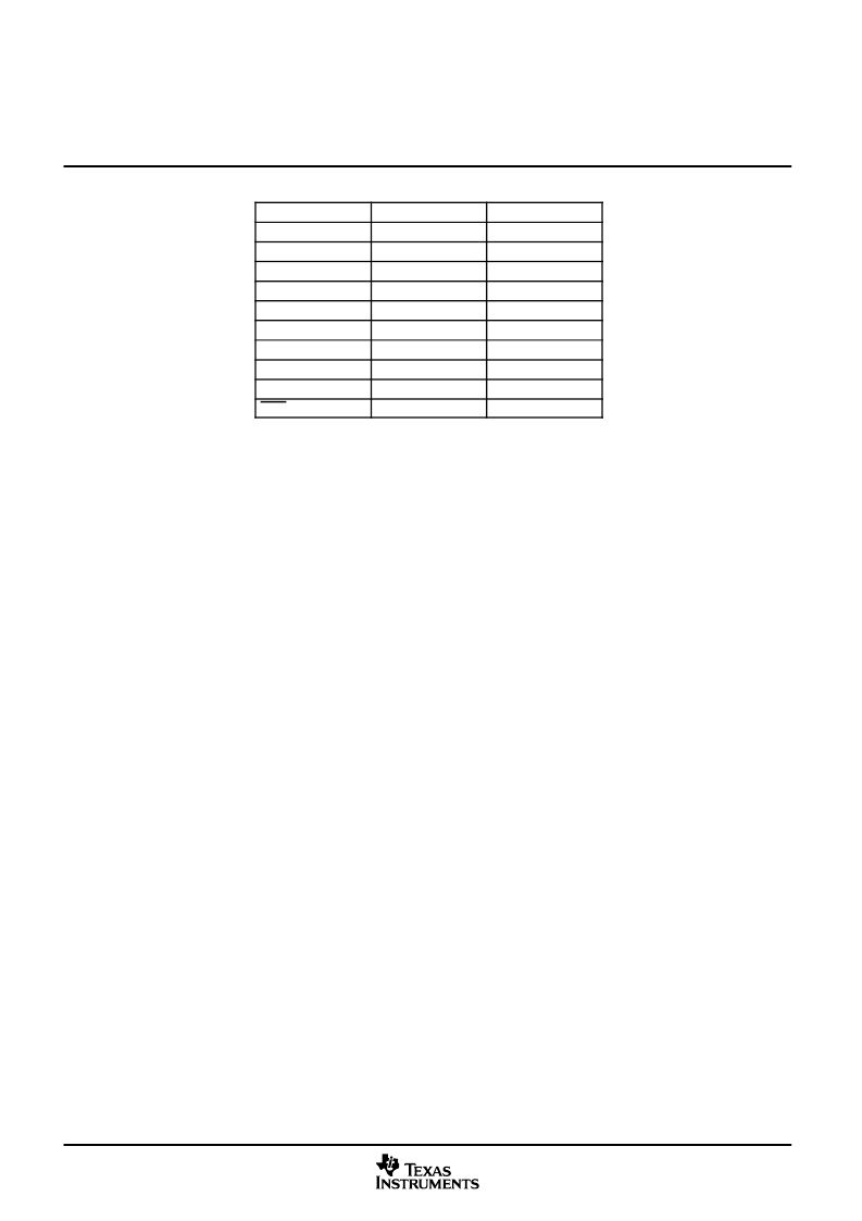
11. Device Outputs During Error Recovery
SIGNAL
MODE
SIGNAL STATE
Valid 1
–
Valid 6
All
Low
PWM P-outputs
All
Low
PWM M-outputs
All
Low
MCLKOUT
All
Low
SCLK
Master
Low
SCLK
Slave
Signal input
LRCLK
Master
Low
LRCLK
Slave
Signal input
SDA
All
Signal input
CLIP
All
High
The transitions are done using a quiet entrance and exit sequence to prevent pops and clicks.
2.4.3 Individual Channel Error Recovery
Individual channel error recovery is used to provide error management and to permit the PWM output to be
turned off. Error recovery is initiated by setting one or more of the six error recovery bits in the error recovery
register to low.
While the error recover bits are brought low, the valid signals goes to the low state. When the error recovery
bits are brought high, a delay of 4 ms to 5 ms occurs before the channels are returned to normal operation.
The delay between the falling edge of the error recover bit and the falling edge of valid 1 though valid 6 is
selectable. This delay can be selected to be either 6
μ
s or 47
μ
s.
The TAS5036 controls the relative timing of the pseudo-differential drive control signals plus the valid signal
to minimize the production of system noise during error recovery operations. The transitions to valid low and
valid high are done using an almost quiet entrance and exit sequence to prevent pops and clicks.
2.4.4 PWM DC-Offset Correction
An 8-bit value can be programmed to each of the six PWM offset correction registers to correct for any offset
present in the output stages. The offset correction is divided into 256 intervals with a total offset correction of
±
1.56% of full scale. The default value is zero correction represented by 00 (hex). These values can be
changed at any time through the serial control interface.
2.4.5 Inter-Channel Delay
An 8-bit value can be programmed to each of the six PWM inter-channel delay registers to add a delay per
channel from 0 to 255 clock cycles. The delays correspond to cycles of the high-speed internal clock, DCLK
(or alternatively the external PLL clock frequency). Each subsequent channel has a default value that is N
DCLKs larger than the preceding channel. The default values are 0 for the first channel and 16 for each
successive channel.
These values can be updated upon power up through the serial control interface. This delay is generated in
the PWM block with the appropriate control signals generated in the CTL block.
These values can be changed at any time through the serial control interface. The optimum performance of
the TAS5036 can be achieved using an interchannel delay of 21.
2.4.6 ABD Delay
A 5-bit value is used to delay the A PWM signals with respect to B PWM signals. The value is the same for
all channels. It can be programmed from 0 to 31 DCLK clock cycles. The default values is 11 DCLK clock cycles
(01011). This value is mask programmable. These values can be changed at any time through the serial
control interface.
The optimum performance of the TAS5036 can be achieved with an ABD delay of 30.
相關(guān)PDF資料 |
PDF描述 |
|---|---|
| TB1239BF | Bi-CMOS Integrated Circuit Silicon Monolithic |
| TB1240AN | PAL/NTSC 1CHIP (IF + VCD RPOCESSOR) IC |
| TB1245N | TOSHIBA Bi-CMOS INTEGRATED CIRCUIT SILICON MONOLITHIC |
| TB1261F | TOSHIBA BiCMOS INTEGRATED CIRCUIT, SILICON MONOLITHIC |
| TB1262F | TOSHIBA BiCMOS INTEGRATED CIRCUIT, SILICON MONOLITHIC |
相關(guān)代理商/技術(shù)參數(shù) |
參數(shù)描述 |
|---|---|
| TAS5036IPFCRG4 | 功能描述:音頻 DSP Digital Audio PWM Processor RoHS:否 制造商:Texas Instruments 工作電源電壓: 電源電流: 工作溫度范圍: 安裝風(fēng)格: 封裝 / 箱體: 封裝:Tube |
| TAS5036PFC | 制造商:TI 制造商全稱(chēng):Texas Instruments 功能描述:SIX CHANNEL DIGITAL AUDIO PWM PROCESSOR |
| TAS5036PFCR | 制造商:TI 制造商全稱(chēng):Texas Instruments 功能描述:SIX CHANNEL DIGITAL AUDIO PWM PROCESSOR |
| TAS5066 | 制造商:TI 制造商全稱(chēng):Texas Instruments 功能描述:SIX-CHANNEL Digital Audio PWM Processor |
| TAS5066-5111D6EVM | 功能描述:音頻 IC 開(kāi)發(fā)工具 TAS5066-5111D6 EVAL MOD RoHS:否 制造商:Texas Instruments 產(chǎn)品:Evaluation Kits 類(lèi)型:Audio Amplifiers 工具用于評(píng)估:TAS5614L 工作電源電壓:12 V to 38 V |
發(fā)布緊急采購(gòu),3分鐘左右您將得到回復(fù)。